Welcome visitor you can login or create an account.

$0.00


News
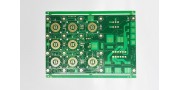
Key Considerations in 4-Layer PCB Prototyping and Design
Optimize 4-layer PCB design by ensuring proper stack-up, power integrity, impedance matching, via placement, and trace length control.
>> Read more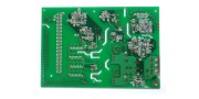
Optimizing PCB Ground Grid for ESD Protection
Optimizing PCB ground grids reduces ESD risks by enhancing return paths, mitigating EMI, and ensuring robust signal integrity.
>> Read more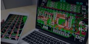
PCB DFM: Design for Better Manufacturability
Optimize PCB manufacturability with DFM: reduce cost, enhance yield, and improve reliability.
>> Read more


Powered by PCBYES