Welcome visitor you can login or create an account.

$0.00
News
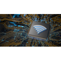
RF PCB Routing for Enhanced Wireless Comm. Performance
The essence of efficient wireless communication relies on rigorous RF PCB routing principles that encompass impedance management, trace optimization, minimal crosstalk, strategic layer allocation, smooth bends, grounding/shielding, component placement, anDate added 27/09/2024
Read more
Distinctions: Plated-Through VS Via Holes in PCB Design
Exploring the critical differences between plated-through holes (PTHs) for electrical connectivity and via holes for component anchoring in PCB design.Date added 26/09/2024
Read more
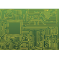
PCB Minimum Distances between Wires and between Wire and Holes
Minimum distances between wires and distances between holes and wire are explained and necessity of the minimum distances is illustrated.Date added 28/08/2024
Read more
-200x200.png)
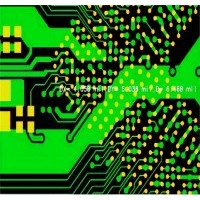
Misunderstandings for PCB Differential Signal Design
Three misunderstandings for PCB differential signal design are introduced, and replies and explanations are given for better understanding.Date added 27/08/2024
Read more
-200x200.jpg)
PCB Wiring
This article mainly discusses general requirements for wiring.Date added 21/08/2024
Read more


Powered by PCBYES