Welcome visitor you can login or create an account.

$0.00
News
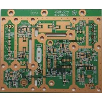
PCB Design Spacing Requirements
PCB design requires careful attention to spacing, which can be categorized into electrical and non-electrical safety. Electrical spacing includes trace-to-trace, pad-to-pad, and copper-to-edge distances, ensuring proper signal integrity, avoiding short ciDate added 06/11/2024
Read more
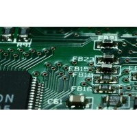
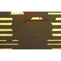
PCB Surface Finishes: Immersion Gold, Electrolytic Gold, HASL
In PCB manufacturing, surface finish treatment is crucial for copper conductor protection, soldering performance enhancement, and electrical property improvement. Popular methods include immersion gold (ENIG), electrolytic gold plating, and hot air solderDate added 04/11/2024
Read more
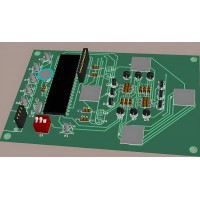
Unveiling PCB Layer Intricacies
This guide unveils the intricacies of PCB layers, crucial for designing and fabricating high-quality PCBs. It covers signal, power, ground, solder mask, silkscreen, and additional layers like mechanical, keep-out, and internal planes, all playing unique rDate added 31/10/2024
Read more
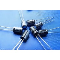
Six Core Functions of Capacitors in PCBs
Capacitors in PCBs serve six main functions: filtering noise, coupling signals, bypassing high-frequency signals, storing energy, controlling timing, and tuning circuits. Selecting and placing capacitors correctly is essential for ensuring circuit performDate added 30/10/2024
Read more
Multilayer PCB Manufacturing Challenges & Controls
Multilayer PCBs, with 10-20+ layers, face manufacturing challenges and are widely used in high-tech fields. Domestic production is mainly by foreign-owned or select domestic firms. Key challenges include interlayer alignment, inner layer circuit fabricatiDate added 28/10/2024
Read more


Powered by PCBYES