
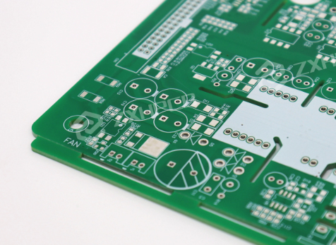
Printed Circuit Boards (PCBs) are essential components in electronic devices, providing both physical support and electrical interconnections for electronic components. From household appliances to advanced aerospace equipment, PCBs are omnipresent. Their manufacturing process involves multiple intricate steps, each critical to the final product's performance and quality.
1. Design Phase
The PCB manufacturing process starts with the design phase. Professional circuit design engineers use Electronic Design Automation (EDA) software, such as Altium Designer and Cadence Allegro, to transform circuit schematics into PCB layouts. During this process, engineers must consider parameters like board dimensions, shape, layer count, and component placement to optimize electrical performance, heat dissipation, and mechanical strength. Compliance with industry standards, such as those set by IPC (Association Connecting Electronics Industries), ensures reliability and manufacturability. With over five years of experience in PCB prototyping and fabrication, PCBYES excels in delivering high-quality PCB design and manufacturing solutions.
2. Material Preparation
Once the design is finalized, the next step is preparing the necessary materials. The fundamental material is the core, typically a copper-clad laminate made from FR-4 (epoxy fiberglass), known for its excellent insulation, heat resistance, and mechanical strength. For multilayer PCBs, prepreg (partially cured epoxy resin sheets) is used for interlayer bonding. PCBs requiring specific properties, such as high-frequency circuits, may incorporate advanced materials like Rogers laminates.
3. Manufacturing Phase
a. Copper Cladding
The initial step in PCB fabrication is copper cladding, where a thin copper foil is laminated onto the core's surface. For double-sided PCBs, copper foils are laminated on both sides. Copper deposition methods include electroplating and electroless deposition. In electroplating, the PCB serves as the cathode in a copper salt solution, where copper ions are deposited onto the surface under an electric field. In electroless deposition, a chemical reaction forms a copper layer without requiring an electric field. Copper thickness typically ranges from 18 to 70 micrometers, depending on design specifications.
b. Etching
Etching is a critical step in forming circuit patterns. A photosensitive layer is first applied to the copper-clad board, and the circuit pattern is transferred onto this layer through photolithography. The board is then immersed in an etching solution, which removes unprotected copper, leaving behind the desired conductive traces, pads, and vias. Common etching solutions include ferric chloride and cupric sulfate. Precise control over etchant concentration, temperature, and exposure time is essential to maintaining pattern accuracy and integrity.
c. Drilling
Drilling creates vias for electrical connections between PCB layers. Using precision drilling equipment, holes ranging from 0.1mm to 3mm in diameter are bored according to the design. Proper drill bit selection, speed control, and cooling techniques prevent overheating and damage to the board.
d. Plating
Plating enhances conductivity and solderability by depositing a uniform metallic layer onto the via walls and circuit traces. Common plating materials include copper, nickel, and gold. Electroplating is conducted in specialized plating solutions, where parameters like solution composition, temperature, and current density determine the plating thickness and quality. Typical plating thicknesses range from 1 to 30 micrometers, depending on the application.
e. Solder Mask Application
Solder mask application forms a protective layer that prevents unintended solder bridges and shields the PCB from environmental damage. Liquid Photoimageable (LPI) solder mask ink is applied evenly over the PCB surface. Using photolithography, the solder mask pattern is transferred onto the ink, and unexposed portions are removed after development. The solder mask layer thickness typically ranges from 20 to 50 micrometers and must ensure strong adhesion without defects like bubbles or particles.
f. Silkscreen Printing
Silkscreen printing involves adding reference indicators, pad labels, and trace markers to the PCB surface. Using precision silkscreen techniques, ink is transferred onto the PCB to create clear, durable markings. The ink used is highly resistant to wear and chemical corrosion to maintain legibility throughout the PCB’s lifecycle.
g. Cutting
Cutting separates individual PCBs from the manufacturing panel. Precision cutting equipment, such as V-cutters or routers, is used to shape the PCB according to design requirements. Ensuring smooth and accurate cuts is essential for maintaining structural integrity and facilitating assembly.
4. Testing Phase
After fabrication, rigorous testing ensures that the PCB meets design and performance specifications.
- Electrical Testing: Verifies conductivity, insulation, and impedance parameters.
- Functional Testing: Simulates real-world operational conditions to ensure proper functionality.
- Environmental Testing: Assesses reliability under conditions such as high temperatures, humidity, and extreme environments.
Through comprehensive testing, manufacturers can identify defects and make necessary adjustments to enhance overall product quality and reliability.
In summary, PCB manufacturing is a complex, precision-driven process requiring stringent quality control and process management. As technology advances, the industry continuously innovates to meet evolving requirements. With a commitment to quality, reliability, and customer satisfaction, PCBYES is dedicated to providing world-class PCB and PCBA services tailored to diverse industry needs.


