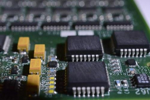
Observing the Insulation Layers:
Principle: Multilayer PCBs incorporate insulation layers between conductive layers to prevent short circuits.
Procedure: Carefully examine the PCB; if you observe one or more intermediate white layers (insulation), you can estimate the number of layers. For instance, a single insulation layer typically indicates a 2-layer board, while two insulation layers suggest a 4-layer PCB. However, this method becomes less reliable for higher-layer-count PCBs.
Assessing the Via and Blind Via Structures:
Principle: Different PCB layer configurations utilize varying via structures for electrical connectivity.
Procedure: For a standard 4-layer PCB, signal traces primarily occupy the top and bottom layers, and the vias fully penetrate the board. In contrast, higher-layer-count PCBs (e.g., 6-layer or 8-layer designs) often employ blind vias, which do not pass through the entire board but only connect specific internal layers. Observing via structures can indicate the PCB's layer count. If all vias penetrate the PCB completely, it is likely a 4-layer board. If some vias terminate within the board, the PCB likely has a higher layer count. However, this approach requires a solid understanding of design patterns in various PCBs.
Using a Light Source and Via Inspection:
Principle: Shining a light through the PCB and analyzing how vias interact with the illumination can reveal the number of layers.
Procedure: Place the PCB over a strong light source, such as a smartphone flashlight, and inspect the vias. If the vials are visible on both sides and no significant shadowing is observed, the board is likely a 2-layer PCB. If vias are only partially visible or shadowing occurs, indicating internal copper layers obstructing the light, it suggests a multilayer PCB. The complexity of the shadowing pattern and the distribution of vias can offer further clues regarding the layer count, but this method depends heavily on experience and familiarity with different PCB stack-ups.
Experience-Based Identification:
Principle: Familiarity with common PCB designs allows engineers to estimate layer counts based on routing complexity and component layout.
Procedure: By observing the trace density and component placement, experienced engineers can make educated guesses about the PCB's layer count. For instance, simple circuit designs typically require only 2-layer PCBs, while more intricate designs demand additional layers for proper signal integrity, power distribution, and EMI shielding. Certain industry-standard PCB layouts can also provide clues about the layer configuration. However, this method lacks precision and relies on extensive industry experience.
With more than 5 years in the field of PCB prototype and fabrication, PCBYES is committed to delivering high-quality, cost-effective solutions to customers across various industries. Our expertise in PCB stack-ups and via structures enables us to provide accurate layer assessments and tailored PCB solutions.
Understanding PCB layer configurations is essential for selecting the right board for a given application. Engineers can quickly determine PCB layer counts by leveraging insulation layer observation via structure analysis, light source techniques, and experience-based assessments, leading to informed design and manufacturing decisions.
PCBYES takes pride in offering PCBA turnkey services, ensuring that our clients receive the best quality products and support. Our dedicated team of electronics engineers is always ready to assist with PCB analysis and manufacturing, making us your reliable partner in every aspect of PCB and PCBA needs.


