
Crosstalk is a critical concept in high-speed PCB design that engineers must understand. It is a primary pathway for electromagnetic interference (EMI) and can cause malfunctions in circuits or components, particularly affecting asynchronous signal lines, control lines, and I/O traces.
What is Crosstalk?
Crosstalk occurs when electromagnetic coupling induces an unwanted voltage noise onto adjacent signal traces. This interference results from mutual inductance and capacitance between traces. Several factors influence crosstalk, including PCB layer parameters, trace spacing, electrical characteristics of the driver and receiver, and termination methods.
Key Strategies to Minimize Crosstalk
To effectively reduce crosstalk, engineers can implement the following measures:
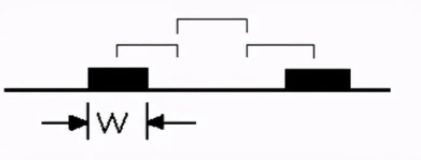
Increase Trace Spacing – Following the 3W rule ensures minimal interference. When the center-to-center distance between adjacent traces is at least three times the trace width, approximately 70% of the electric field interference is mitigated. For even better isolation (98%), a 10W spacing can be applied. However, in real-world PCB designs, achieving 10W spacing is often impractical.
Insert Grounded Shielding Traces – Placing grounded traces between parallel signal lines can significantly reduce crosstalk by providing a return path for the signal.
Reduce the Distance Between Traces and Ground Plane – Lowering the separation between signal layers and the ground plane helps to minimize the loop area, thereby reducing the noise.
Best Practices for Crosstalk Reduction in PCB Layout
To prevent crosstalk, engineers should adopt strategic PCB layout and design practices, such as:
- Categorizing Functional Blocks – Logical components should be grouped based on their function to maintain a structured bus topology.
- Minimizing Component Distances – Keeping components physically close to each other helps in reducing unwanted coupling.
- Separating High-Speed Signals – High-speed signals and critical components (e.g., oscillators) should be placed away from I/O ports and sensitive areas prone to coupling.
- Proper Signal Termination – Ensuring correct termination reduces signal reflections and prevents signal integrity issues.
- Avoiding Long Parallel Traces – Signal traces should not run parallel for extended distances. Maintaining adequate spacing minimizes inductive coupling.
- Routing Adjacent Layers Perpendicularly – When using microstrip or stripline configurations, traces on adjacent layers should be routed perpendicularly to each other to reduce capacitive coupling.
- Reducing Trace-to-Ground Distance – This minimizes the impact of unwanted signal interference.
- Isolating High-Noise Signals – Noisy elements like clocks, I/O, and high-speed interconnects should be placed in separate PCB layers to reduce EMI.
- Maximizing Signal Trace Spacing – Keeping signal traces apart effectively reduces capacitive crosstalk.
- Minimizing Lead Inductance – Avoiding circuits with extremely high or low impedance loads is essential. High-impedance loads increase capacitive crosstalk, while low-impedance loads increase inductive crosstalk.
- Routing High-Speed Signals in Inner Layers – Placing critical high-speed signals within PCB inner layers reduces EMI radiation and provides shielding.
- Implementing Impedance Matching – Proper impedance matching maintains signal integrity, preventing overshoot and further reducing crosstalk.
- Ground Shielding for Fast-Edge Signals – Signals with a fast rise time (tr ≤ 1ns) should be enclosed by ground traces to prevent crosstalk.
- Using Ground Planes – A continuous ground plane provides a return path for signals, offering 15-20dB attenuation compared to designs without one.
- Employing Differential Pairs and Shielding – Balanced lines, shielded cables, or coaxial lines effectively mitigate crosstalk.
- Filtering Noise Signals – Applying filters to interference-prone and sensitive traces helps in noise suppression.
- Optimizing PCB Stackup and Trace Layout – Proper stackup design, adjusting trace spacing, and reducing parallel trace lengths significantly minimize crosstalk.
By following these best practices, PCB designers can effectively mitigate crosstalk, ensuring reliable signal integrity in high-speed, high-density PCB layouts. At PCBYES, we specialize in designing and fabricating high-performance PCBs with optimized layouts that adhere to industry standards, minimizing signal interference while maximizing functionality.
With more than five years of expertise in PCB prototyping and fabrication, PCBYES is committed to delivering high-quality solutions tailored to meet the needs of various industries. Whether you require turnkey PCBA services or custom PCB designs, our skilled team ensures optimal performance with precision engineering and dedicated customer support.


