
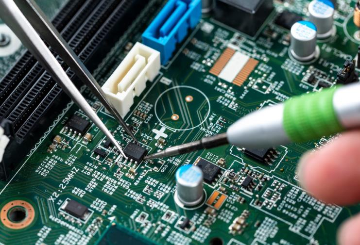
In the process of PCB assembly (PCBA), soldering quality plays a crucial role in determining the overall product quality, making it a key factor that requires close attention. The primary causes of soldering defects on PCB boards can generally be categorized into three main areas: the solderability of PCB vias, PCB warpage, and PCB design.
1. Solderability of PCB Vias Affects Soldering Quality
Poor solderability of PCB vias can lead to cold solder joints, which can severely affect the performance of components on the circuit board. This, in turn, leads to unstable connections between multilayer board components and internal circuitry, ultimately causing functional failures within the entire system.
Solderability refers to the ability of a metal surface to be wetted by molten solder, forming a uniform, continuous, and smooth thin film of adhesion. A solderable surface promotes better solder joint formation and improves overall soldering efficiency.
Several factors influence the solderability of a printed circuit board (PCB):
• Solder Composition and the Nature of the Metal Being Soldered
Solder material is a critical component of the soldering process, consisting of chemical materials containing flux. The commonly used low-melting-point eutectic metals are Sn-Pb (tin-lead) or Sn-Pb-Ag (tin-lead-silver). The impurity levels must be controlled within certain limits to prevent oxidation, which would otherwise interfere with the soldering process. Flux plays a vital role in transferring heat and removing rust from the surface, facilitating better wetting of the PCB. Common fluxes used include rosin and isopropyl alcohol as solvents.
• Soldering Temperature and Surface Cleanliness
The temperature at which soldering occurs significantly impacts solderability. When the temperature is too high, the solder’s diffusion rate increases, causing the circuit board and solder surface to oxidize quickly, resulting in soldering defects. PCB surface contamination also affects solderability, leading to defects such as solder balls, open circuits, poor gloss, and more.
2. Warpage-Induced Soldering Defects
PCB and component warpages can cause various soldering defects, including cold solder joints, open circuits, and short circuits, primarily due to stress deformation during the soldering process. Warpage typically occurs due to temperature imbalances between the top and bottom sides of the PCB. Larger PCBs may experience warpage due to the board's weight, further complicating the soldering process.
For instance, in typical PBGA (plastic ball grid array) components, there is a 0.5mm gap between the component and the PCB. If the components are large, during the cooling phase, the PCB will attempt to return to its original shape, but this can exert long-term stress on the solder joints, possibly leading to issues such as virtual solder joints or open circuits. Even a slight lift of 0.1mm in the component can result in a cold solder joint.
3. Design of the PCB Affects Soldering Quality
The design of the PCB is another critical factor influencing soldering quality. A PCB that is too large can make soldering easier in some cases, but it can increase the length of printed traces, increase impedance, and reduce noise immunity, leading to increased costs. On the other hand, very small PCBs can result in poor heat dissipation, difficulty controlling soldering, and the risk of interference between adjacent traces, leading to electromagnetic interference (EMI) and other design-related problems.
To ensure high-quality soldering and reliable functionality, it is essential to optimize the PCB design, including:
• Reducing Trace Length for High-Frequency Components
Minimizing trace length between high-frequency components reduces EMI interference, improving performance.
• Supporting Heavier Components
For components heavier than 20g, it is advisable to mount them using supports before soldering to ensure stability and prevent warping.
• Thermal Management for Heat-Generating Components
It is essential to consider thermal management, especially for heat-sensitive components. Heat-generating components should be placed away from sensitive areas to avoid creating thermal gradients (ΔT) that could lead to defects and rework.
• Optimizing Component Layout
The arrangement of components should be as parallel as possible, not only for aesthetic purposes but also for ease of soldering, especially in mass production. A 4:3 aspect ratio for PCB design is considered ideal. It is crucial to avoid abrupt changes in trace width to prevent discontinuities in the routing, which could lead to problems during the soldering process. Additionally, when a PCB is subjected to prolonged heat exposure, copper foil can expand and detach, so using excessive copper foil should be avoided to mitigate this risk.
At PCBYES, we understand the importance of addressing soldering issues in PCB manufacturing and assembly. With over 5 years of experience in PCB prototype and fabrication, we are committed to delivering high-quality, reliable solutions that cater to our customers' diverse needs. Our experienced electronics engineers are equipped to provide comprehensive PCBA turnkey services, ensuring that all soldering-related challenges are addressed effectively.
We take pride in our customer-centric approach, working closely with clients to provide timely support, ensuring optimal design and production solutions, and maintaining the highest standards in soldering and quality assurance. Whether you're dealing with solderability issues, PCB warpage, or design-related challenges, PCBYES is your trusted partner in achieving flawless PCBs and PCBA solutions.


