
1. Consider the Choice of Component Package
During the schematic design phase, decisions related to component packages and pad patterns should be made, as these will directly impact the layout stage. Below are some important points to consider when selecting components based on package type:
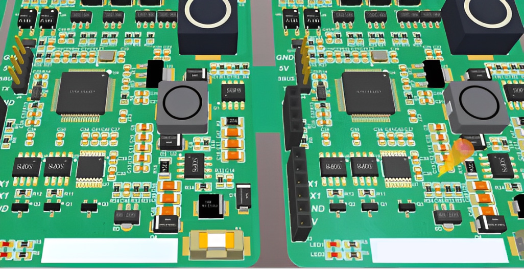
(1) Keep in mind that the package involves both the electrical pad connections and the mechanical dimensions (X, Y, and Z), which refer to the shape of the component and its pins that connect to the PCB. When selecting components, it's important to consider any mounting or packaging restrictions on the PCB's top and bottom layers. Some components, such as polarized capacitors, may have height clearance limitations, which should be factored into the selection process. At the initial design stage, it's recommended to sketch a basic outline and place key components (such as large or placement-critical components). This allows for an intuitive and quick view of the PCB's virtual layout (without traces) and gives a fairly accurate representation of the relative positioning and component heights. This can help ensure that components will fit into their enclosures (plastic casing, chassis, etc.) after assembly. You can easily browse the entire PCB in 3D preview mode from the tool menu.
(2) The pad pattern displays the actual pad or via shape used for soldering components on the PCB. These copper patterns also include some basic shape information. The correct pad dimensions are crucial to ensure proper soldering and the mechanical and thermal integrity of the connected components. When designing the PCB layout, it’s important to consider how the PCB will be manufactured or how it will be hand-soldered. Reflow soldering (where the flux is melted in a controlled high-temperature oven) can handle a wide variety of surface-mount devices (SMDs). Wave soldering is typically used to solder the opposite side of the PCB to secure through-hole components but can also handle some surface-mount components placed on the backside. In wave soldering, bottom-side SMDs often need to be placed in a specific orientation, and pad modifications may be necessary to accommodate this method.
(3) The component selection can change throughout the design process. It is helpful to decide early on which components will use plated through-hole (PTH) and which will use surface-mount technology (SMT) to optimize the overall PCB layout. Factors to consider include component cost, availability, area density, and power consumption. From a manufacturing perspective, SMT components are typically cheaper than through-hole components and are generally more available. For small and medium-scale prototype projects, it's best to select larger SMT or through-hole components, as these are easier to solder by hand and facilitate better debugging and connectivity during testing.
(4) If a package is not available in the component database, custom packages can generally be created within the tools.
2. Use Proper Grounding Methods
Ensure the design includes adequate bypass capacitors and a ground plane. When using capacitors, it’s critical to place the appropriate decoupling capacitors close to the power and ground pins (preferably on the ground plane). The appropriate capacitance depends on the application, capacitor technology, and operating frequency. Placing bypass capacitors between the power and ground pins, and ensuring they are positioned correctly relative to the IC pins, can optimize the circuit's electromagnetic compatibility (EMC) and susceptibility.
3. Assign Virtual Component Packages
Print a Bill of Materials (BOM) to verify virtual components. Virtual components do not have associated packages and will not pass on to the layout phase. Create a BOM and review all virtual components in the design. The only items should be power and ground signals, as these are considered virtual components and are treated separately in the schematic environment, not transferring to the layout design. Unless used for simulation purposes, components shown as virtual should be replaced with those that have associated packages.
4. Ensure You Have Complete BOM Data
Check that the BOM report contains enough complete data. After generating the BOM report, carefully review it, ensuring that all incomplete component entries are filled in, including details such as the component’s manufacturer, supplier, and part numbers.
5. Sort Components Based on Their Reference Designators
To make the BOM easier to sort and review, ensure that the component reference designators follow a continuous numbering scheme.
6. Inspect for Redundant Gates
Generally, all unused gates should have their inputs connected to signals, preventing floating inputs. Ensure that all extra or missing gate circuits are checked and that any inputs not connected to signals are properly grounded. In some cases, an IC with floating pins may not function correctly. For example, in dual operational amplifier ICs where only one op-amp is used, it is recommended to either utilize the second op-amp or connect its input pins to the ground, along with an appropriate feedback network to ensure the IC functions correctly.
In some cases, ICs with floating pins may fail to work within specifications. This occurs because the IC or other gates within the same device may not be operating in their specified range when the inputs or outputs are near or at the power rails. Simulation typically cannot capture these effects, as the simulation model generally does not simulate the floating connections across multiple gates.


