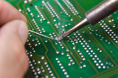
Welding is a fundamental metal-joining process that plays a critical role in various industries, including PCB (Printed Circuit Board) manufacturing. However, one significant challenge associated with welding is welding deformation, which can severely affect the final product's quality and functionality. Ensuring that the post-weld workpiece meets specific standards requires implementing effective methods to control these deformations. This article introduces some commonly used methods for controlling welding deformation, particularly in the context of PCB manufacturing.
► Preheating and Post-Weld Heat Treatment:
Preheating is the process of heating the workpiece to a specific temperature before welding. This method is particularly beneficial in reducing the temperature gradient during the welding process, minimizing the chances of deformation. In some cases, post-weld heat treatment can further reduce deformation. This process involves reheating the welded workpiece and holding it at a specific temperature for a set period, allowing internal stresses to be released and reducing the likelihood of deformation. Both preheating and post-weld heat treatment are essential techniques to ensure the PCB's integrity and reliability after welding, particularly in more complex designs.
► Use of Proper Fixtures and Positioning Tools:
During the PCB manufacturing process, it's essential to ensure that the workpiece remains stable and positioned correctly throughout the welding process. Using the appropriate fixtures and positioning tools helps maintain the PCB's alignment, thus reducing the potential for deformation. Proper fixtures limit the degrees of freedom during welding, ensuring that the workpiece remains in its desired position. Additionally, correct positioning ensures that welding joints are accurate, reducing the need for future corrections, and ultimately enhancing the overall quality of the assembled PCB.
► Controlling Welding Parameters:
Welding parameters such as current, voltage, welding speed, and the selection of welding materials all play a significant role in the deformation process. By selecting and adjusting these parameters effectively, it's possible to reduce the heat input, thereby minimizing the risk of deformation during welding. At PCBYES, we take great care in ensuring that the welding parameters for our PCBs and PCBA projects are optimized to achieve the best possible results. Using appropriate soldering materials and fillers also improves the quality of the welding process and reduces the chance of deformation.
► Welding Sequence:
The sequence in which welding is performed is another crucial factor in controlling deformation. By adopting a well-planned welding sequence, it’s possible to reduce thermal accumulation and stress concentration, which are major contributors to deformation. Generally, welding from the inside to the outside, or from the center to the outer edges, can help minimize deformation. This is particularly important for larger PCBs and assemblies, where even slight misalignments can affect the overall performance.
► Process Monitoring and Control:
Modern welding technologies allow for real-time monitoring of welding parameters and quality throughout the process. By using technologies such as lasers, visual sensors, and automated control systems, any issues that arise during welding can be detected and adjusted immediately, reducing the risk of deformation. PCBYES incorporates advanced monitoring systems into its production process, ensuring that each PCB or PCBA undergoes continuous quality checks to meet the highest standards. This real-time monitoring and feedback system significantly enhances the overall welding quality and process efficiency.
► Post-Weld Heat Treatment:
In some cases, the welded workpiece may require additional post-weld heat treatment to eliminate residual stress and reduce deformation. Heat treatments such as normalizing, tempering, and annealing are commonly used in the welding industry to refine the properties of welded materials. By precisely controlling the heat treatment parameters, manufacturers can minimize the effects of welding deformation, resulting in a higher-quality final product. This step is especially important in complex or high-precision PCB designs, where even minor deviations can lead to functionality issues.
► Use of Compensating Components:
When designing and manufacturing welded components, including PCBs, it’s possible to incorporate compensating parts that can be adjusted post-weld to counteract deformation. This approach is commonly used in cases where welding deformation is inevitable, particularly when producing large-scale structures or components with intricate shapes. The addition of compensating components allows for adjustments after the welding process, ensuring that the final product meets the desired specifications.
Welding deformation is a common and significant issue in the PCB manufacturing process. However, by employing the methods outlined above, manufacturers can effectively control deformation and ensure that the final product meets the required standards for quality and performance. At PCBYES, we are committed to providing top-notch PCBs and PCBA solutions while minimizing defects and deformation throughout the entire production process. Our experienced engineers and state-of-the-art technology enable us to deliver high-quality products that meet the demands of customers across various industries.
In real-world applications, welding engineers and PCB manufacturers must consider these techniques in combination to achieve optimal welding results. By implementing proper preheating, controlling welding parameters, and using advanced monitoring systems, the risk of deformation can be significantly reduced. This results in more reliable and accurate PCBs, ultimately benefiting the end-user by ensuring long-term performance and durability.


