
In any switching power supply (SMPS) design, the physical design of the PCB is the final step. If the design approach is incorrect, the PCB may emit excessive electromagnetic interference (EMI), leading to instability in the power supply operation. Below, we analyze key considerations for each step of the design process.
At PCBYES, we understand how critical these considerations are, and with over 5 years in PCB prototype and fabrication, we ensure high-quality designs that meet all your specifications and requirements.
1. Design Flow from Schematic to PCB
The typical design process from schematic to PCB layout involves the following steps:
- Establish component parameters
- Input schematic netlist
- Set design parameters
- Manual placement
- Manual routing
- Design Verification
- Review
- CAM output
At PCBYES, our experienced engineers assist in every step of the design flow, ensuring the highest standards of quality and efficiency.
2. Design Parameter Settings
The spacing between adjacent traces must meet electrical safety requirements. For ease of operation and manufacturing, the trace spacing should be as wide as possible. The minimum spacing must at least withstand the expected voltage. When routing is sparse, the signal trace spacing can be increased. For signal traces with large voltage differences (high and low-level signals), it is important to keep the traces short and increase the spacing. Typically, a trace spacing of 8 mils is used.
The distance from the inner hole edge of the pad to the edge of the PCB should be greater than 1mm to avoid pad damage during processing. When routing fine traces connected to pads, the connection between the pad and the trace should be designed in a "teardrop" shape. This design reduces the risk of pad lifting and ensures that the pad and trace remain securely connected.
3. Component Placement
Even if the circuit schematic is correct, improper PCB layout can adversely affect the reliability of the electronic device. For example, if two fine parallel traces are too close, signal waveform delays may occur, and reflections at the transmission line terminals can create noise. Improper grounding and power plane routing can also result in interference, reducing product performance. Therefore, it is crucial to adopt the correct design methods when designing the PCB.
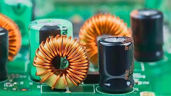
A switching power supply typically has four current loops:
- Power switch AC loop
- Output rectifier AC loop
- Input signal source current loop
- Output load current loop
An approximate DC charges the input capacitor, and the filter capacitor primarily serves as wideband energy storage. Similarly, the output filter capacitor stores high-frequency energy from the output rectifier and eliminates DC energy in the output load loop. Hence, the connection points for the input and output filter capacitors are critical. The input and output current loops should connect only through the capacitor's terminals. If the connection between the input/output loop and the power switch/rectifier loop cannot directly connect to the capacitor’s terminal, AC energy will be radiated to the environment through the input or output filter capacitors.
The power switch AC loop and the rectifier AC loop carry high-amplitude trapezoidal currents. These currents have a high harmonic component, with frequencies much higher than the switching frequency. The peak amplitude can be up to five times the steady-state input/output DC, and the transition time is typically around 50ns. These two loops are the most likely sources of electromagnetic interference (EMI), so it is essential to route these AC loops before any other PCB traces. The three primary components in each loop—filter capacitors, power switches or rectifiers, and inductors or transformers—should be placed close together, and their current paths should be as short as possible.
4. Optimized Layout Process
The best approach for switching the power supply layout is similar to its electrical design. The optimal design process is as follows:
- Place the transformer.
- Design the power switch current loop.
- Design the output rectifier current loop.
- Connect the control circuit to the AC power circuit.
- Design the input current source loop and input filter.
- Design the output load loop and output filter.
At PCBYES, our team specializes in optimized layouts to minimize loop areas, reduce EMI, and improve the overall efficiency and reliability of the switching power supply.
When arranging components, it is essential to consider the following principles:
- PCB Size: PCB dimensions must be chosen carefully. A large PCB results in longer trace lengths, increased impedance, decreased noise immunity, and higher manufacturing costs. A small PCB, on the other hand, may lead to poor heat dissipation and increased susceptibility to interference. The optimal PCB shape is rectangular, with an aspect ratio of 3:2 or 4:3. Components placed near the edge of the PCB should maintain at least a 2mm distance from the board's edge.
- Component Placement: Ensure sufficient space for future soldering and avoid overly dense component placement.
- Functional Unit Layout: The core components of each functional unit should be placed at the center, with components arranged uniformly, neatly, and compactly on the PCB. This minimizes trace lengths and simplifies connections. Decoupling capacitors should be placed as close as possible to the VCC pin of the components.
- High-Frequency Circuits: For circuits operating at high frequencies, consider the parasitic effects of the components. It is generally better to arrange components parallel to each other. This improves aesthetics, eases soldering, and facilitates mass production.
- Signal Flow and Layout: Arrange components according to the signal flow, ensuring that signal directions remain consistent to avoid unnecessary signal reflections.
- Routing Efficiency: The primary goal of the layout is to ensure high routing efficiency. Minimize trace lengths and organize components to avoid excessive “flying” traces (unconnected traces that traverse long distances). Place related components together to simplify connections.
- Minimize Loop Area: Reduce the loop area as much as possible to suppress EMI in the switching power supply.
By following these guidelines and leveraging the expertise of PCBYES, you can achieve a more efficient PCB design, minimizing EMI and enhancing the performance of your power supply.


