
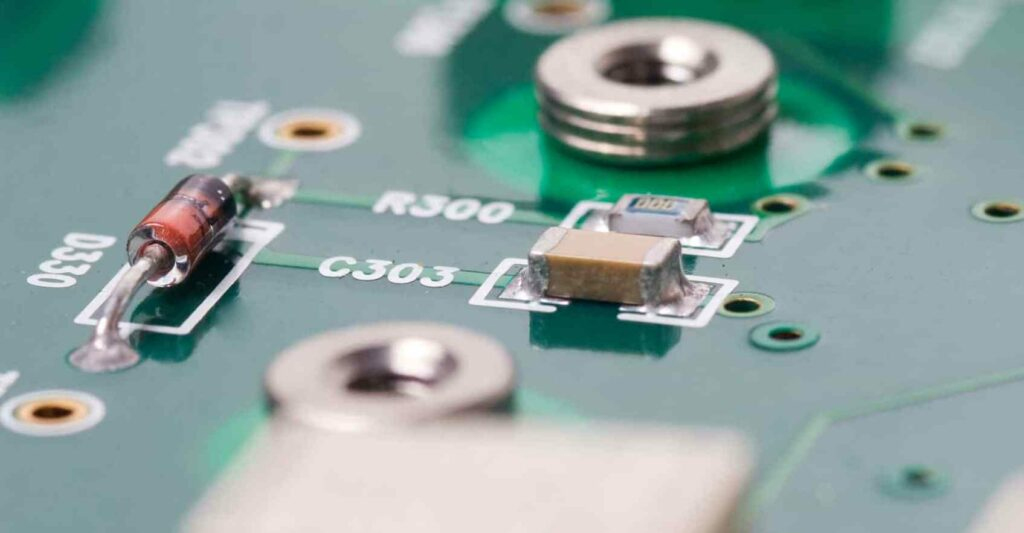
In printed circuit board (PCB) production, via holes (also known as vias) are critical for creating electrical connections between layers. To meet customer requirements, these vias often need to be plugged. Through extensive experimentation and practice, traditional aluminum plug methods have been replaced by white mesh technology, which integrates the PCB's surface solder mask and via hole plugging. This has led to stable production and reliable quality.
Via holes play an essential role in connecting circuit paths across layers in a PCB. As the electronics industry evolves, it has driven the development of PCBs to become more complex, dense, and multi-layered, which in turn demands higher manufacturing standards for PCB production processes and surface-mount technologies (SMT). This led to the emergence of via hole plugging, which must meet the following criteria:
- Copper in the Via Hole: The via hole should contain copper, but plugging the hole with a solder mask is optional.
- Solder and Lead Requirements: The via hole must have a specific amount of solder (around 4 microns) inside, with no solder mask ink entering the hole that could cause solder balls to form inside.
- Via Hole Plugging: The via hole must be plugged with a solder mask, ensuring that it is opaque, free of solder rings, and solder balls, and remains smooth.
At PCBYES, we are committed to meeting your PCB requirements—whether it’s high-quality production, timely delivery, cost-effectiveness, or addressing any specific needs. Our expertise in via hole plugging plays a significant role in ensuring the integrity of your PCBs, as it helps prevent several common issues:
- Preventing Solder Bridges: Via hole plugging prevents solder from flowing through the via during wave soldering, especially when vias are placed under BGA pads. Plugging the vias ensures better BGA soldering by avoiding solder bridges.
- Avoiding Flux Residue: Plugging helps prevent flux residues from remaining inside the via, which can cause issues in later stages of production.
- Vacuum Test Requirements: For final testing of PCBs after SMT assembly, vacuum formation is necessary, which can be affected by unplucked vias.
- Preventing Solder Paste Leakage: Plugging via holes prevents solder paste from entering the holes, which could lead to dry solder joints.
- Preventing Solder Balls: Via hole plugging reduces the risk of solder balls ejected during wave soldering, which could lead to short circuits.
Via Hole Plugging Process
For surface-mount boards, particularly for BGAs and ICs, the via holes need to be plugged in such a way that they are smooth and level, with a tolerance of ±1 mil. The process should prevent issues like solder creeping up the edges of the via and creating solder balls. The via-plugging process can be complex, involving multiple steps, and the control is difficult, as issues like ink droplet leakage and oil blowouts during curing can occur.
Here, we summarize the main via plugging processes, comparing their steps and advantages/disadvantages:
1. Via Plugging After Hot Air Leveling (HAL)
The typical process flow via plugging after HAL includes:
- Solder Mask Application
- Hot Air Leveling (HAL)
- Via Plugging
- Curing
In this method, a mesh screen or stencil made from aluminum is used to fill the vias with a solder mask. The plugging ink can be photosensitive or thermoset ink, and the same ink used for the surface mask is preferred to maintain consistency. This method ensures that no ink falls off during hot air leveling, but it can cause contamination on the surface, leading to unevenness, which can cause issues in SMT, particularly in BGA placement.
At PCBYES, we are equipped with the latest technologies to ensure minimal surface contamination, and our skilled team ensures that HAL does not affect the quality of via hole plugging.
2. Via Plugging Before Hot Air Leveling
There are two common methods for plugging before HAL:
Using Aluminum Sheets to Plug Vias: CNC drilling machines create the aluminum stencils, and the via holes are plugged using ink. This method ensures a full plug, but it requires thickened copper plating to ensure adequate copper thickness around the walls. The process involves pre-treatment, via plugging, plate grinding, graphic transfer, and etching.
Screen Printing the Surface Mask After Via Plugging: A similar approach, but with the via plugging occurring first, followed by direct screen printing of the surface solder mask. This method provides more control over ink consistency and thickness, but after curing, there may still be issues with soldering pad coverage, leading to poor solderability.
3. Pre-cure Plugging, Grinding, and Masking
In this method, the via is plugged using an aluminum stencil, followed by pre-curing, grinding, and then final surface solder mask application. This method provides a smooth, high-quality finish, preventing issues like oil blowouts and solder ball formation. However, the process still faces challenges with solder coverage in the via holes, and not all manufacturers can meet the strict copper thickness requirements.
4. Simultaneous Solder Mask and Via Plugging
In this process, screen printing of both the surface solder mask and via plugging is completed at the same time, ensuring efficient use of equipment. While this method shortens processing time and increases equipment utilization, it can lead to issues with trapped air in the via holes, which could cause incomplete curing or uneven filling of the vias.
Via hole plugging is a crucial process in PCB manufacturing, especially with the increasing complexity and density of modern PCB designs. Each via-plugging method has its strengths and limitations, and selecting the right one depends on the design’s specific needs. At PCBYES, we offer expertise and advanced solutions to ensure the highest-quality PCB production. Our commitment to quality, cost-effectiveness, and timely delivery makes us a trusted partner in your PCB and PCBA (Printed Circuit Board Assembly) needs.
By ensuring proper via hole plugging, we help prevent a range of potential issues like solder bridges, flux residues, and solder ball formation, ultimately providing you with more reliable and functional PCBs. Whether you need complex multilayer PCBs or standard designs, PCBYES is here to be your best business partner, offering solutions tailored to your unique requirements.


