1. Why Should PCB Traces Not Be Too Long?
Printed Circuit Boards (PCBs) are critical in electronic devices, connecting and supporting electronic components. Traces are the conductive pathways that interconnect circuits. Overly long PCB traces can lead to several issues, including:
- Signal Attenuation: Signals transmitted through traces are subject to attenuation. Longer traces increase the likelihood of signal loss, which can cause distortion, noise, and communication errors. This is particularly problematic for high-frequency and high-speed signals.
- Signal Delay: Signals take time to propagate through a circuit. Long traces increase this propagation delay, which can degrade performance or even lead to system failure in applications like high-speed communication or timing-sensitive circuits.
- Crosstalk Interference: Longer traces increase the chances of crosstalk interference, where a signal on one trace induces interference in adjacent traces. This can lead to errors or noise in the circuit.
- Layout Challenges: Excessively long traces can complicate PCB layout, making it difficult to manage factors like signal paths, power distribution, and component placement.
To mitigate these problems, it is essential to keep PCB traces as short as possible through effective circuit layout, trace routing, and the use of appropriate interconnections.
2. Increased Parasitic Capacitance with Longer Traces

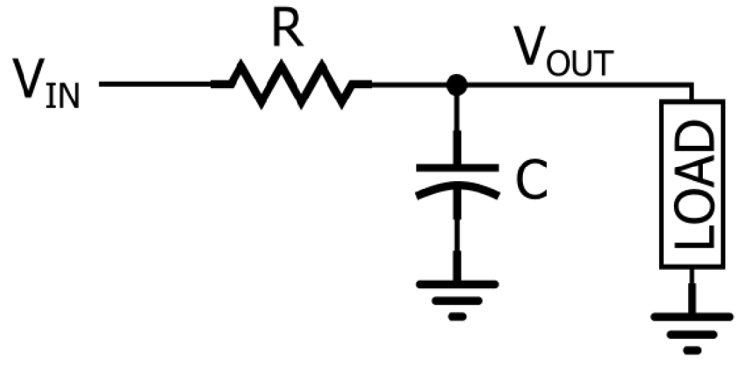
Longer PCB traces result in greater parasitic capacitance. Without delving into microscopic analyses, capacitance increases with the surface area between conductive planes, assuming the spacing remains constant. Longer traces create larger effective areas, increasing the overall capacitance.
Higher capacitance acts as a low-pass filter, attenuating high-frequency components. This degradation can impact signal integrity, particularly for high-speed circuits. Designers must consider this factor when planning trace lengths and layouts.
3. Increased Parasitic Inductance with Longer Traces
Long PCB traces also increase parasitic inductance. The inductance of a trace is proportional to its length. Key contributors to parasitic inductance include:
- Trace Length: As length increases, the inductance increases proportionally.
- Trace Width and Thickness: Wider and thicker traces reduce inductance by offering greater conductor surface area and cross-sectional area.
- Trace Shape and Layout: Zigzagging, coiled, or tightly spaced traces increase inductance. Proximity to other traces or conductors also exacerbates this effect.
Parasitic inductance can degrade circuit performance by slowing signal transmission, introducing crosstalk, and reducing bandwidth. Optimizing trace dimensions and layouts is essential to controlling parasitic inductance.
4. Optimizing Trace Length via Layout
Proper PCB layout is foundational for reducing trace lengths. Effective layout involves:
- Functional and Modular Design: Place components in groups based on functionality to minimize interconnections and trace lengths.
- Balanced and Aesthetic Design: Ensure a uniform component distribution to avoid dense or unbalanced layouts.

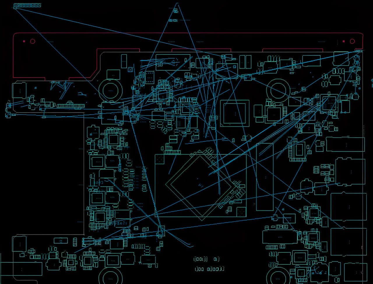
Tools like "rat’s nest" lines (unrouted connection indicators) assist in evaluating the shortest connection paths between components. By rotating and repositioning components, designers can identify the most efficient trace paths.
5. Why Use Serpentine Traces Despite Short-Trace Preference?
Serpentine (zigzag) traces are sometimes used to ensure signal timing accuracy. In digital circuits, signal transitions between high and low levels require time for stabilization. To maintain proper setup and hold times at the receiving end, traces are lengthened as necessary to match timing constraints. Key concepts include:
- Setup Time (Tsu): The minimum time data must be stable before the clock edge.
- Hold Time (Th): The minimum time data must remain stable after the clock edge.
Failure to meet these timing requirements can lead to metastable outputs, causing unpredictable circuit behavior. Serpentine traces are still relevant in specific parallel interfaces like DDR, where timing synchronization is critical. However, modern serial interfaces like PCIe, USB, and SATA have reduced the reliance on these designs. In high-speed serial designs, attention shifts to signal quality metrics like eye diagrams.


