
Inductors are essential components in electronic circuits. They are found in various types and configurations, each tailored to specific applications. Understanding their structure, characteristics, and handling techniques is crucial in PCB design, particularly to optimize performance and mitigate potential electromagnetic interference (EMI).
Basic Structure of Inductors
An inductor typically consists of two main components: the winding and the core.
- Winding: The winding comprises conductive coils, usually made of copper or aluminum wires. The cross-sectional area and the number of turns in the coil determine the inductance. Windings may be arranged in single or multi-layer configurations, with parallel or interleaved patterns.
- Core: The core can be made from various materials such as air, solid magnetic materials, or magnetic powder. The choice of core material significantly influences the inductor’s performance by enhancing its magnetic flux. Commonly used materials include iron, nickel, and ferrite.
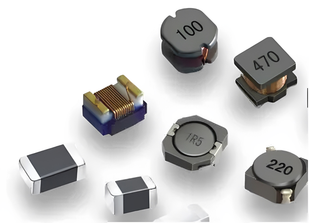
Inductors may vary in internal structure depending on their application and manufacturing process. For instance, iron-core inductors use ferromagnetic materials, while others like SMD (surface-mount device) inductors are designed for compactness and efficiency. Auxiliary components, such as damping capacitors or protective sleeves, may also be included to enhance circuit performance and protect the inductor.
Power Inductors and Their Applications
Among various types, power inductors are commonly encountered in PCB design. These can be classified into two types: shielded and unshielded. The primary distinction lies in visibility; shielded inductors conceal their windings within a metal casing, whereas unshielded inductors do not.
Power inductors play a critical role in power electronics, serving as integral components in AC/DC converters, DC/DC converters, filter networks, and voltage regulators. Their key functions include:
- Filtering: Power inductors provide an impedance to the load circuit, effectively separating high-frequency and low-frequency signals. They are crucial in smoothing the output waveforms of power supplies, reducing ripples, and stabilizing the voltage.
- Transient Response: Power inductors manage transient responses in power supplies, controlling phenomena like inrush currents and current pulses. This improves system stability and prevents overcurrent conditions.
- Energy Storage: In AC/DC and DC/DC converters, power inductors store energy in their magnetic field and release it as electrical energy, providing a higher current or voltage over a short period.
- Isolation: By isolating the input power source from the output section, power inductors reduce electromagnetic interference (EMI) and noise coupling, improving circuit reliability.
Power inductors are vital for mitigating ripple, addressing current overloads, and enhancing stability in power electronics applications.
Managing Inductors in PCB Design
During PCB design, handling inductors requires careful attention due to their generation of magnetic fields, which vary with time and can interfere with surrounding electronic components. This interference may degrade circuit performance, causing issues such as signal noise or instability.
To minimize interference, the following measures are commonly implemented:
- Copper Clearance: One standard practice is removing copper traces around the inductor. The magnetic field generated by the inductor can couple with nearby copper traces, leading to EMI. By clearing copper in the vicinity, the magnetic field’s spread is reduced, lowering its impact on surrounding components.
- Shielding: Placing a shielding cover around the inductor confines the magnetic field within a defined area, further reducing EMI. Shielded inductors inherently achieve this effect due to their design, making them a preferred choice for high-density PCB layouts.
- Thermal Management: Inductor magnetic fields can induce eddy currents in nearby copper traces if clearance is inadequate. These currents generate heat and reduce inductance, potentially impairing circuit performance. Proper copper removal or perforations in shielding areas above power inductors can help mitigate eddy current effects.
- Layout Optimization: Strategic placement of inductors on the PCB helps minimize interference. Separating inductors from sensitive components and employing low-noise power supplies or grounding techniques can further reduce EMI.
- Choosing Shielded Inductors: In scenarios where space constraints or performance requirements are critical, shielded inductors are advantageous. Their magnetic field is confined within the shielding material, effectively reducing interference with adjacent components.
Addressing Eddy Currents and EMI in PCB Design
If copper traces are left intact around the inductor, the interaction between the inductor’s magnetic field and the copper can generate eddy currents. These currents not only cause heating in the region but also reduce the inductance value, impairing circuit efficiency.
When using shielded enclosures in PCB design, it’s essential to consider ventilation or perforations in areas surrounding power inductors. This prevents eddy current formation and ensures optimal thermal dissipation.
Key Takeaways for PCB Design
To effectively handle inductors in PCB design, focus on the following:
- Pay close attention to the layout of the inductor region, ensuring sufficient copper clearance to reduce EMI.
- Incorporate shielding techniques for inductors to limit magnetic field exposure to nearby components.
- Use shielded inductors when EMI reduction is a priority, as their design inherently minimizes interference.
- Optimize circuit layouts to maintain a balance between performance, space, and thermal management.
- By adopting these practices, designers can minimize EMI effects, ensure circuit stability, and create reliable PCB systems. Power inductors, with their critical role in power electronics, demand particular care in design to achieve optimal performance and efficiency.


