
The layout of components on a PCB is crucial for both functional and aesthetic reasons. A well-structured layout makes the board visually neat and significantly impacts the length and number of conductive traces, ultimately influencing the entire system's performance. Effective PCB component placement plays a vital role in enhancing overall system functionality.
1. Key Points for PCB Layout with Wireless Modules
- Separation of Analog and Digital Circuits: Ensure physical separation between analog and digital circuits. For instance, keep the MCU and the antenna ports of the wireless module as far apart as possible.
- Placement Below Wireless Modules: Avoid placing high-frequency digital traces, high-frequency analog traces, power supply traces, or other sensitive components directly beneath the wireless module. Instead, use copper pours under the module.
- Electromagnetic Interference Considerations: Wireless modules should be positioned far from transformers, high-power inductors, power supplies, or other sources of electromagnetic interference.
- Antenna Clearance: For modules with onboard or ceramic PCB antennas, ensure the PCB below the antenna area is clear of copper and features cutouts. Place the antenna section close to the PCB edge.
- Signal Routing: Keep RF and other signal traces as short as possible. Other signal traces should maintain adequate distance from the RF transmission section to minimize interference.
- Power and Ground Considerations: Ensure the wireless module has a continuous power ground, and allocate space for ground vias along RF traces.
- Voltage Ripple and Filtering: Wireless modules demand low voltage ripple. Place suitable filtering capacitors (e.g., 10 μF) near the module's voltage input pins.
- Power Transient Response: Wireless modules require robust transient power response. Use high-performance power supply designs and optimize power circuit layout. For example: In DC-DC layouts, minimize the distance between the rectifier diode ground and IC ground to ensure proper current return paths. Keep the distance between power inductors and capacitors as short as possible.
2. Trace Width and Spacing Configuration
Proper configuration of trace width and spacing has a substantial impact on PCB performance. Optimized settings enhance electromagnetic compatibility (EMC) and overall system reliability.
Power Trace Width: Determine the trace width based on factors such as current load, supply voltage, PCB copper thickness, and trace length. For instance, a 1.0 mm wide, 1 oz (0.035 mm) copper trace can typically carry approximately 2 A of current.
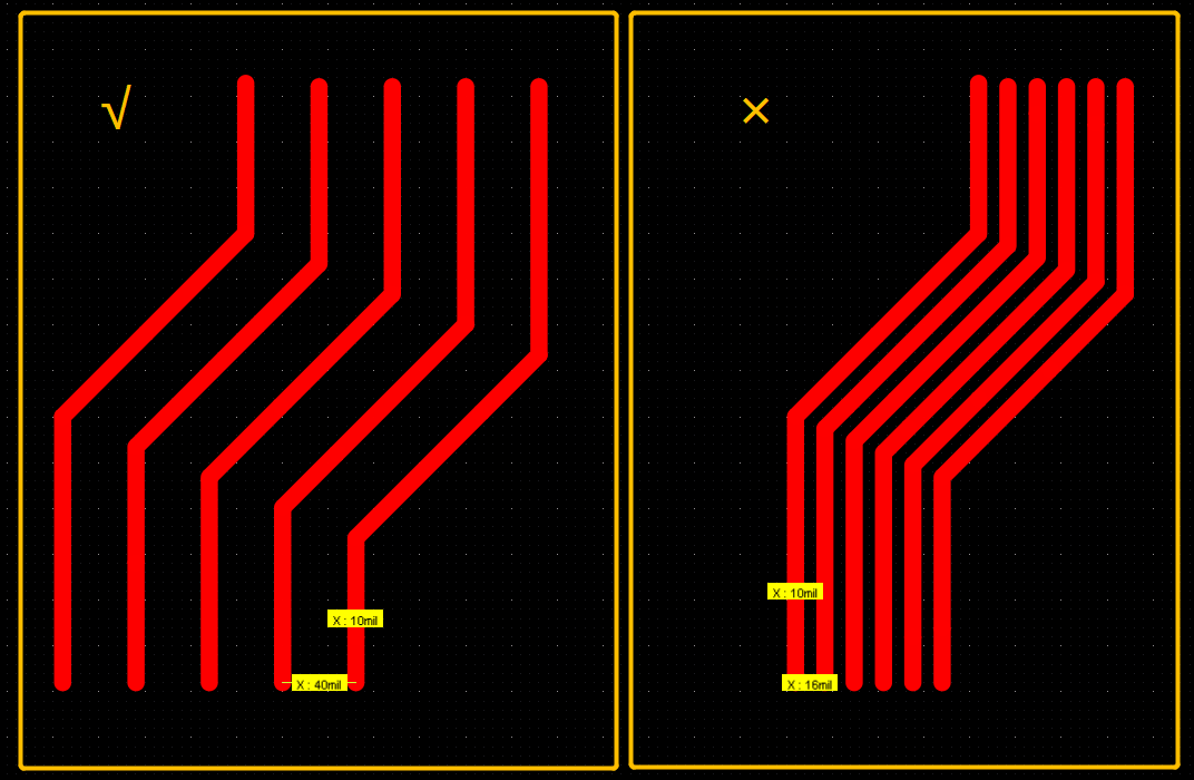
Trace Spacing: Adhering to the "3W rule" (trace spacing ≥ three times the trace width) reduces electromagnetic interference, maintaining up to 70% field separation. Spacing of 10× trace width reduces crosstalk by up to 95%.
Specific Recommendations:
- Power Traces: Account for load current, voltage, and copper thickness. Allow a safety margin by designing for twice the normal operating current. Adhere to the 3W rule for spacing.
- Signal Traces: Base spacing on signal speed, transmission type (analog or digital), and trace length. The 3W rule is a common guideline for regular signals, while differential pairs require separate considerations.
- RF Traces: Design RF traces with characteristic impedance in mind. For example, a 50 Ω trace for RF modules can be achieved with a 0.55 mm trace width and 0.5 mm spacing from adjacent copper. For precise impedance, consult with the PCB manufacturer.
3. Component Spacing Guidelines
Maintaining proper spacing between components during PCB layout is critical to ensure manufacturability and avoid defects such as solder bridging.
Spacing Recommendations:
- Same-type components: ≥ 0.3 mm
- Different-type components: ≥ 0.13 × height difference (h) + 0.3 mm
- Hand-soldered components: ≥ 1.5 mm
- Spacing between through-hole and surface-mount components: 1–3 mm
4. Board Edge Clearance for Components and Traces
Proper clearance from the PCB edge is essential to prevent issues during penalization and depaneling, such as pad lifting or component damage.
Component Placement:
- Align component pads parallel to the panel’s "V-cut" direction to distribute mechanical stress evenly during depaneling.
- Maintain a minimum distance of 0.5 mm from the edge.
Trace Clearance:
- Keep traces at least 0.5 mm away from the board edge.
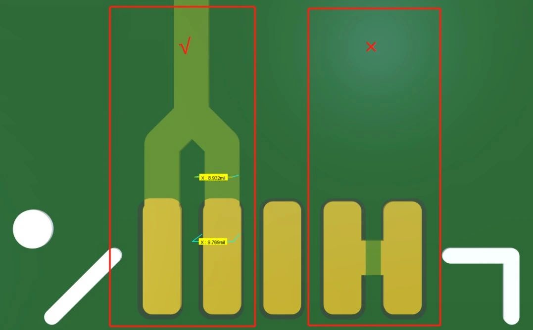
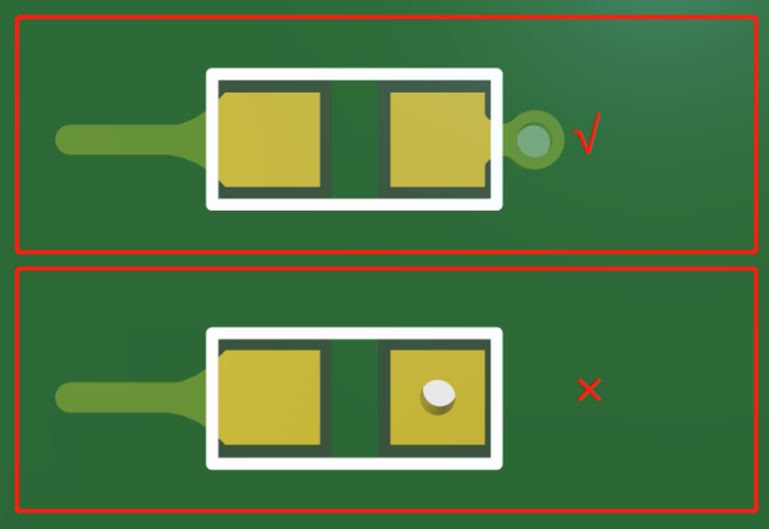
5. Adjacent Pad Connections and Teardrops
When connecting adjacent IC pads, avoid direct pad-to-pad routing. Instead, route traces outside the pad area. This minimizes the risk of solder bridging during manufacturing.
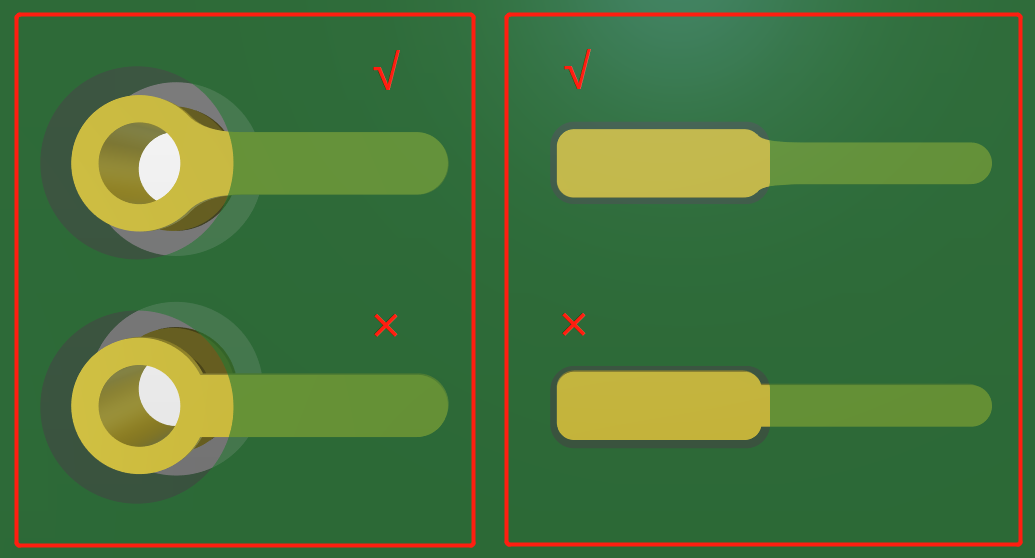
Teardrop Implementation:
- Use teardrops to reduce signal reflection caused by abrupt trace width changes.
- Improve the mechanical strength of the pad-to-trace connection.
- Enhance the PCB’s visual appearance.
6. Via Parameters and Placement
Via size and placement significantly influence circuit performance. Proper design must account for current carrying capacity, signal frequency, and manufacturing constraints.
Key Considerations:
- Limit via sizes to three types per board to avoid production complexity.
- Maintain a depth-to-diameter ratio ≤ 6 to ensure consistent copper plating.
- Pay attention to parasitic inductance and capacitance, particularly for high-speed circuits.
- Smaller vias are preferable for high-frequency signals but incur higher manufacturing costs.
Placement Guidelines:
Avoid placing vias directly on pads to prevent soldering defects unless advanced techniques such as "via-in-pad" are employed with manufacturer support.


