
Pads are an essential concept in PCB design. PCB engineers are very familiar with them, but many may not fully grasp all the details regarding the different types of pads and their design standards. Pads are fundamental components in surface mount assembly, forming part of the land pattern used to create specific pad configurations for various component types.
Pads in PCBs are used for electrical connections, component fixation, or both. Below is an overview of the common types of pads in PCB design and the standards used to design them.
► Types of PCB Pads
1. Common Pads
- Square Pads
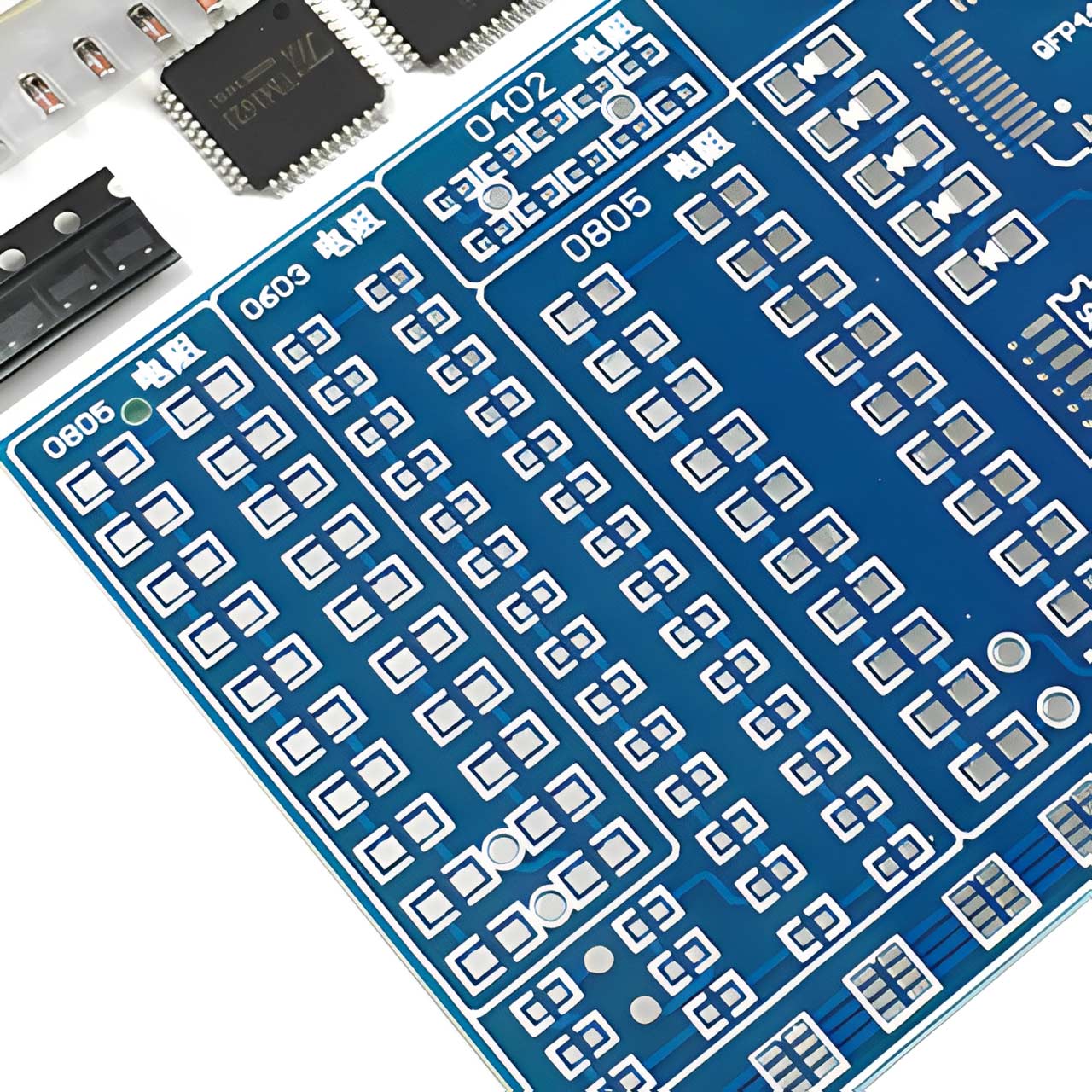
Square pads are commonly used in PCBs with fewer, larger components and simple routing. They are often chosen for handmade PCBs due to their ease of implementation.
- Round Pads
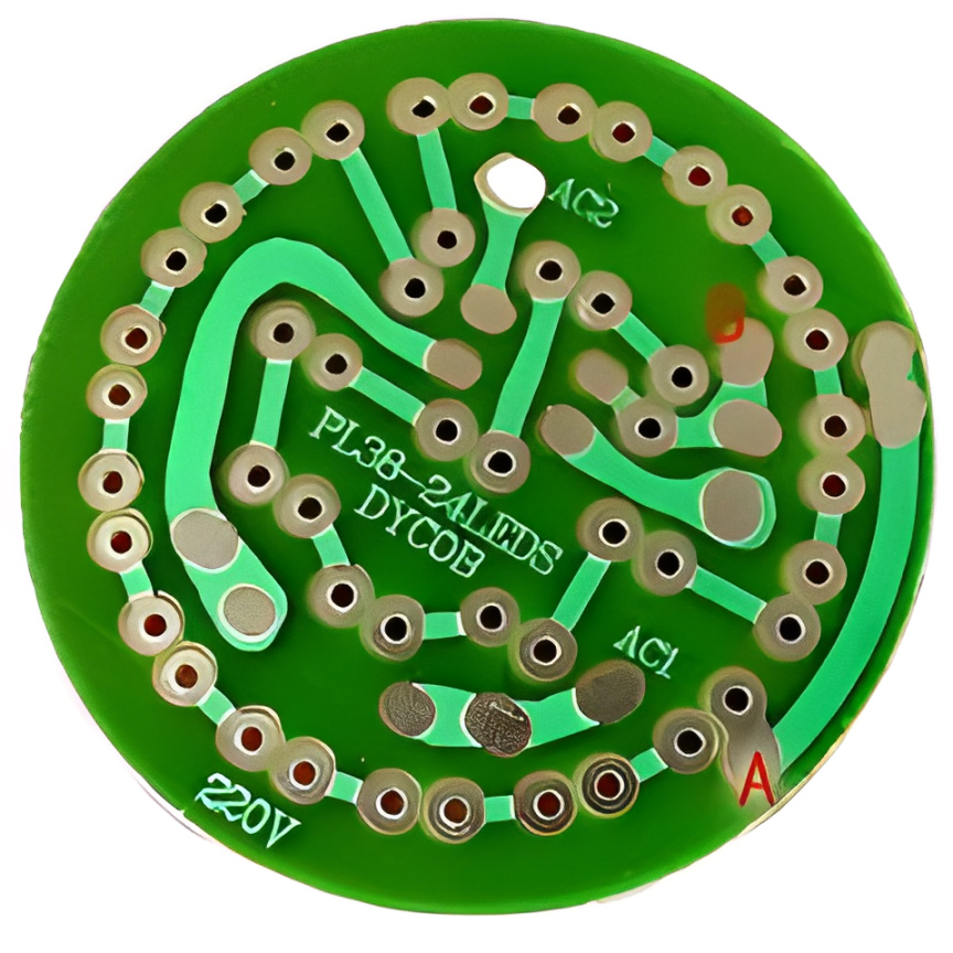
Round pads are widely used in single and double-sided PCBs where components are arranged in a regular grid. If the board density allows, the pads can be larger, making soldering more stable and reducing the risk of pad detachment.
- Island Pads
Island-shaped pads involve connecting the pads through a combined trace, commonly used in installations where components are arranged in an upright or irregular manner.
- Polygon Pads
Polygonal pads are used when the outer diameter of the pad is similar but the hole diameter varies, which facilitates processing and assembly.
- Oval Pads
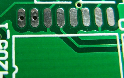
Oval pads are designed to provide sufficient surface area for enhanced peel resistance and are typically used in dual in-line packages (DIP) for through-hole components.
- Slotted Pads
Slotted pads are often used to ensure manual reflow soldering will not block the through-hole after wave soldering. They are designed to allow post-wave soldering repairs without obstruction.
2. Special Pads
- Flower Pad
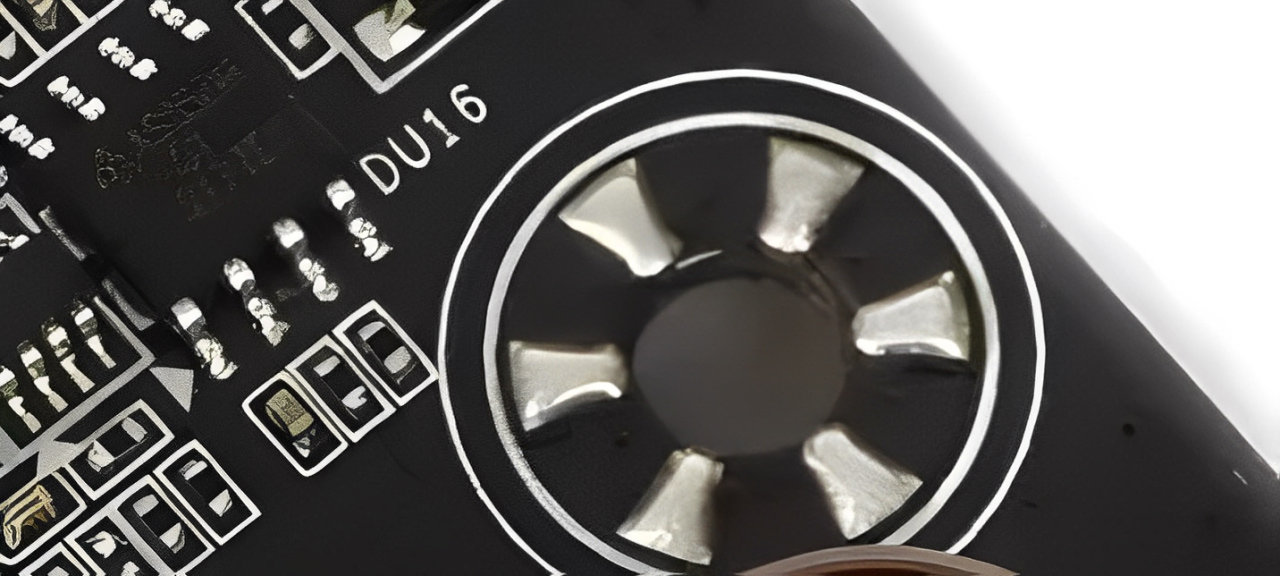
Flower pads are typically used in locations where large via grounding is required. The design is chosen for several reasons:
A fully metalized through-hole might become clogged during reflow soldering, preventing proper grounding.
Using internal threaded holes could lead to poor grounding due to installation or disassembly stress. Flower-shaped pads ensure reliable grounding under varying stress conditions.
- Cross Pad

Also known as thermal or hot-air pads, cross pads are designed to reduce heat dissipation during soldering, preventing issues like cold solder joints or PCB delamination.
When the pad is part of a ground plane, cross pads reduce the area connected to the ground, slowing down heat transfer to facilitate easier soldering.
For PCBs that use automated pick-and-place machines and reflow soldering, cross pads help to prevent PCB delamination, as more heat is required to melt the solder paste effectively.
- Teardrop Pad
Teardrop pads are commonly used when the trace width is thin, preventing pad lifting or disconnection from the trace. These pads are often used in high-frequency circuits to ensure stable connections.
► Design Standards for PCB Pads
1. Shape and Size Design Standards for PCB Pads:
- Use a standardized PCB component library for pad designs.
- The minimum single-sided pad width should not be less than 0.25mm, and the pad diameter should not exceed three times the component hole diameter.
- The gap between the edges of the two pads should be at least 0.4mm.
- For pads with hole diameters exceeding 1.2mm or pad diameters greater than 3.0mm, diamond or flower-shaped pads should be used.
- For dense wiring, it is recommended to use oval or elongated circular pads. The minimum diameter of a single-sided PCB pad should be 1.6mm. For double-sided boards, weak signal pads should have a hole diameter plus an additional 0.5mm. Large pads can lead to unintended solder bridges.
2. PCB Pad Hole Size Standards:

The diameter of the hole in the pad should generally not be smaller than 0.6mm. Holes smaller than 0.6mm can be difficult to process during hole punching. Typically, the inner hole diameter of the pad should be the component lead diameter plus 0.2mm. For instance, if a resistor's lead diameter is 0.5mm, the corresponding pad hole diameter would be 0.7mm. The pad diameter is then determined based on the inner hole diameter.
3. PCB Pad Reliability Design Considerations:
- Symmetry: The pads at both ends of a component should be symmetric to ensure the surface tension of molten solder is balanced.
- Pad Spacing: Pads that are spaced too far apart or too close together can result in soldering defects. Ensure the spacing between the component leads and pads is optimal for proper soldering.
- Remaining Pad Area: After the component leads or pins overlap the pads, the remaining pad area must be large enough to allow the formation of a proper solder joint with a concave shape.
- Pad Width: The width of the pad should generally match the width of the component lead or pin to ensure a reliable solder joint.


