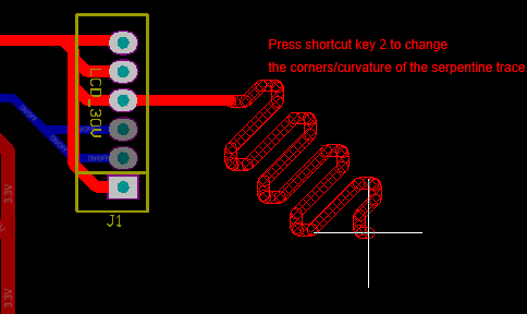
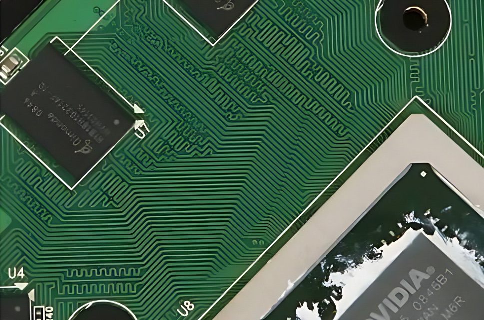
A small PCB (Printed Circuit Board) is often densely populated with hundreds or even thousands of electronic components, all working together to maximize the functionality of the board. Designing the layout of circuits and components requires technical expertise, and one essential technique in PCB design is "snake-shaped routing," which serves a unique and critical role.
When carrying high-frequency signals, every trace on a PCB will introduce a delay to the signal due to the transmission line effect. The main purpose of snake-shaped routing is to compensate for signal delay differences within a group of related signals. Some of these signals typically experience less delay because they may not pass through the same amount of logic processing as others. The most typical example is clock signals, which usually do not pass through additional logic processing and thus experience smaller delays compared to other related signals.
In high-speed digital PCB designs, equal-length traces are crucial to maintaining signal integrity. Equal-length routing ensures that all signals in the group experience similar propagation delays, thus preserving the timing accuracy of the system and preventing errors in data reading. The allowable delay variation is typically less than one-quarter of a clock cycle; otherwise, the system could misread data from the next cycle. The delay between traces depends on several factors, including trace width, trace length, copper thickness, and the layer stack-up. However, excessively long traces can increase the distributed capacitance and inductance, which negatively impacts signal quality.

The role of the clock IC's pins is typically connected with an RC network to minimize delay, but snake-shaped routing does not function as an inductor. On the contrary, inductance can cause phase shifts in higher-order harmonics of the signal's rise time, degrading signal quality. For this reason, the trace spacing in snake-shaped routing should be at least twice the width of the trace. The smaller the rise time of the signal, the more susceptible it is to the effects of distributed capacitance and inductance.
The use of snake-shaped routing varies depending on the application and offers different benefits. In computer motherboard designs, snake-shaped traces are often used as a form of filtering inductance to enhance the board's ability to resist electromagnetic interference. For example, clock signals like CIClk and AGPClk on a motherboard often incorporate snake-shaped traces. The two main purposes of these traces are:
- Impedance matching: Ensuring that the impedance of the trace matches the source and load, which helps prevent signal reflections.
- Filtering inductance: Serving as a filter to improve the signal integrity and reduce noise.
For critical signals, such as those used in the Intel HUB architecture (specifically the HUBLink signal, which operates at 233 MHz), maintaining equal-length traces is vital to avoid timing issues caused by signal delay. A total of 13 traces must be precisely matched in length to eliminate the risk of delay-induced errors. In this case, snake-shaped routing is the only viable solution.
In general, snake-shaped traces should maintain a minimum spacing at least twice the width of the trace. For instance, in PCI boards, snake-shaped routing ensures that trace lengths meet the timing requirements for the PCI 33 MHz clock. In simpler PCBs, snake-shaped traces function as LC filters, and in some cases, they can also serve as inductive components, like radio antenna coils. Narrow, short snake-shaped traces can even act as fuses in some applications.


