What is a PCB Solder Mask?
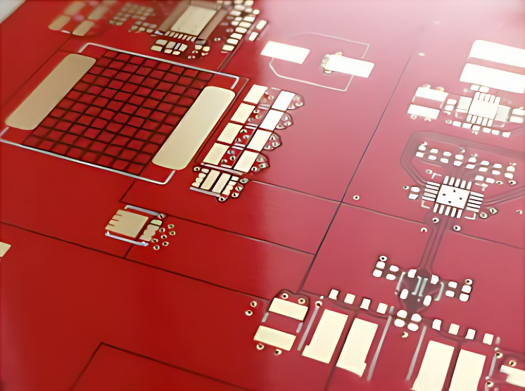
A solder mask is a protective polymer layer applied during the PCB manufacturing process to safeguard the metal elements of the board from oxidation and prevent short circuits caused by solder bridges between pads. This layer is particularly essential when using reflow or wave soldering techniques, which are less precise in controlling the placement of molten solder. The term "solder resist" is also commonly used and might be more accurate since the layer doesn’t involve a literal application of solder to the entire PCB surface.
Types of PCB Solder Mask
All solder masks consist of a polymer layer applied over the metal conductors on a printed circuit board (PCB). The best solder mask type for a specific board depends on cost and application requirements. Basic solder masks use screen printing techniques, where liquid epoxy resin is printed onto the conductors, similar to spraying paint through a stencil. Solder masks are available in a wide range of colors.
► Liquid Epoxy Solder Mask
The simplest and most cost-effective solder mask is liquid epoxy resin applied via screen printing. This method remains one of the most popular options. In this process, a mesh screen supports the ink-blocking pattern. Liquid epoxy is a thermosetting polymer that hardens during thermal curing. Dye is mixed into the epoxy, allowing the mask to cure into the desired color.
► Liquid Photoimageable Solder Mask (LPSM)
Advanced solder masks use a photolithography process, similar to the photolithography used in semiconductor manufacturing, for defining openings in the solder mask for pads, vias, and mounting holes. LPSM can be screen printed like epoxy or sprayed onto the surface for a more economical application. A more precise method involves using photolithography to match the openings to the Gerber file design.
For this process:
- A photo tool is created to match the desired solder mask layout.
- The PCB panel is thoroughly cleaned to ensure no dust particles remain under the cured solder mask.
- Both sides of the panel are fully coated with liquid LPSM.

The solder mask is applied using epoxy resin or photosensitive polymers.
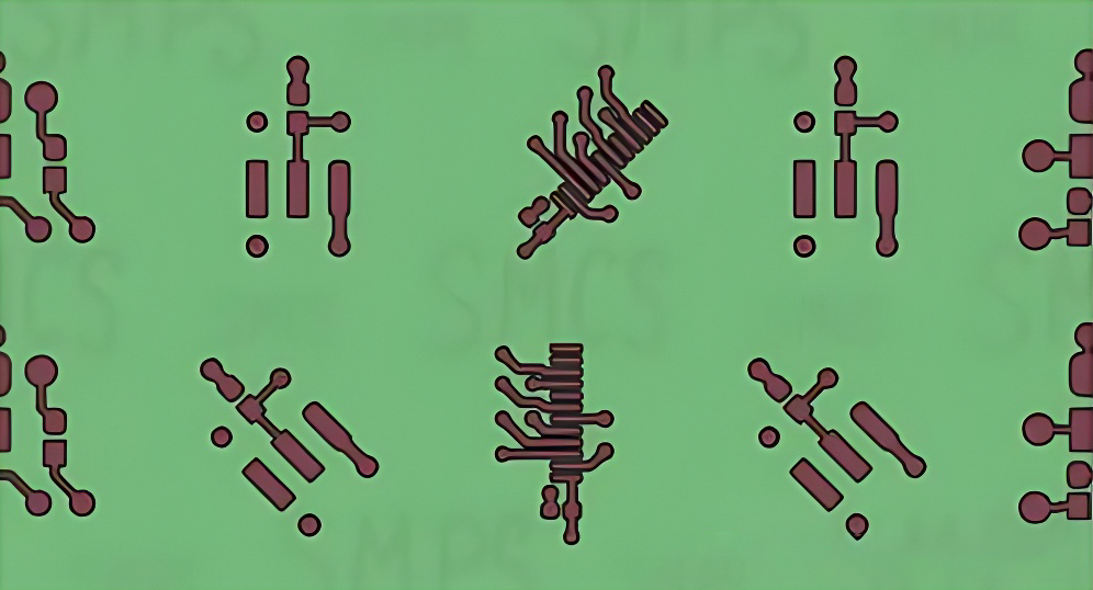
The black areas of the photo tool define regions where conductors are to be exposed, while transparent areas indicate where the solder mask should remain. After coating, the board is pre-dried in an oven, aligned with the photo tool, and exposed to UV light. Exposed areas of the LPSM cure under UV, while unexposed areas are washed away with a solvent, leaving a hardened solder mask.
► Dry Film Solder Mask (DFSM)
Dry film solder masks follow a similar process to LPSM but use a vacuum lamination technique to apply the solder mask as a film instead of a liquid coating. During lamination, the solder mask film adheres to the PCB under vacuum, removing air bubbles from the layer. After exposure to UV light, unexposed areas are washed away, and the remaining film undergoes thermal curing for hardening.
► Topside and Bottomside Solder Masks
In many PCB solder mask guides, references to "topside" and "bottom side" solder masks simply denote their application on the PCB's top or bottom layer. These terms do not specify a manufacturing process or solder mask material type.
Final Steps: Curing and Surface Finish
After applying the solder mask, the PCB undergoes final cleaning to remove dust and particles. The solder mask is then cured and hardened. Liquid epoxy solder masks are thermally cured, while LPSM and DFSM layers undergo UV curing during the photolithography process, followed by heat treatment.
ENIG plating is performed on exposed copper areas through openings in the solder mask
Regardless of the solder mask type, the resulting mask leaves certain copper areas exposed on the PCB. These exposed areas must receive a surface finish to prevent oxidation. Common surface finishes include Hot Air Solder Leveling (HASL), Electroless Nickel Immersion Gold (ENIG), and Electroless Nickel Electroless Palladium Immersion Gold (ENEPIG). Additional openings in the solder mask may also accommodate flux for joining pads or other components to the PCB, depending on the assembly process.


