
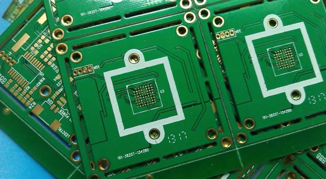
1. What is Copper Pour?
Copper pour, or copper filling, refers to the process of utilizing idle spaces on a circuit board as reference planes and filling them with solid copper. These copper areas are also known as copper pours. The significance of copper pour lies in reducing ground impedance, enhancing anti-interference capabilities, lowering voltage drop, improving power efficiency, and connecting to the ground to minimize loop areas. To prevent PCB deformation during soldering, most PCB manufacturers require designers to fill copper sheets or create grid-like ground patterns in open areas on the PCB. However, improper copper pour can lead to more disadvantages than advantages. Determining whether the benefits of copper pour outweigh its drawbacks depends on various factors.
In high-frequency situations, the distributed capacitance of traces on a printed circuit board becomes significant. When the length of a trace exceeds 1/20 of the wavelength corresponding to the noise frequency, an antenna effect occurs, allowing noise to radiate through the traces. Poorly grounded copper pours in a PCB can act as noise propagation tools. Therefore, in high-frequency circuits, merely connecting a portion of the ground trace to the ground does not constitute a proper ground. Instead, holes should be drilled in the traces at intervals less than λ/20 to ensure good grounding with the ground plane of multilayer boards. Properly handled copper pour not only increases current carrying capacity but also provides dual interference shielding.
2. Two Forms of Copper Pour
Copper pour generally takes two basic forms: large-area copper pour (solid copper fill) and hatch fill (grid-like copper pattern). The debate on which is better—solid copper fill or hatch fill—is not straightforward.
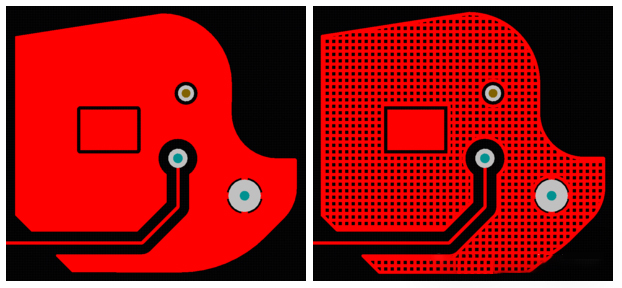
Solid copper fill offers both increased current capacity and shielding effects. However, large-area copper pour can cause the board to warp or bubble during wave soldering. To mitigate copper foil bubbling, slots are often cut into large-area copper pours.
Hatch fill primarily serves a shielding purpose, with reduced current-carrying capacity. From a thermal perspective, hatch fill has benefits (reducing the heated surface area of copper) while also providing electromagnetic shielding. It is particularly useful in touch circuits, as shown below:
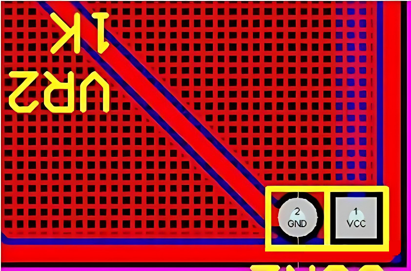
It's worth noting that the grid in the hatch fill is composed of intersecting traces. For circuits, the width of traces has a corresponding "electrical length" related to the board's operating frequency (calculated by dividing the physical size by the numerical frequency corresponding to the operating frequency, as detailed in relevant literature).
When the operating frequency is low, the effect of grid lines may not be significant. However, when the electrical length matches the operating frequency, it can cause severe issues, rendering the circuit unable to function properly and emitting interference signals that disrupt system operation.
The recommendation is to select the appropriate copper pour method based on the specific working conditions of the PCB design. Therefore, high-frequency circuits with high interference resistance requirements often use hatch fill, while low-frequency circuits with high current demands typically use solid copper pour.


