
Introduction: What is a Core Board?
An embedded core board, also known as a System-on-Module (SOM), integrates a CPU and various peripherals, such as memory (DDR), storage (eMMC or FLASH), power management (PMIC), oscillators, and more. It offers interfaces like USB, GPIO, SPI, I2C, UART, Ethernet, and PCIe, catering to diverse applications.
SOMs typically connect to baseboards via board-to-board connectors, stamp hole soldering, gold fingers, or COM Express standards. They expose all or most CPU functional pins, allowing designers to focus only on interface circuit designs based on application needs. This simplifies hardware development and accelerates time to market.
SOMs find applications in industrial automation, medical devices, automotive electronics, communication systems, and IoT. Their modularity significantly shortens development cycles, reduces costs, and improves product reliability.
Classification of Core Boards
To ensure compatibility, modularity, and scalability of hardware and software, various organizations and companies have established multiple standards for embedded core boards. Commonly used standards include:
1. Open Standard Module (OSM):
- Compact LGA solderable modules, with sizes up to 45mm x 45mm.
- Power consumption below 15W, ideal for IoT applications requiring cost-effectiveness and high performance.
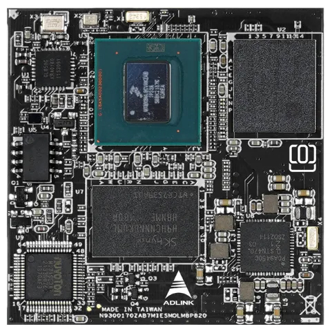
2. QSeven (Q7):
.jpg)
- Introduced by NXP Semiconductors, it is based on ARM architecture.
- Features a 230-pin MXM connector for high-speed I/O connections, suitable for handheld devices, HMIs, and signage applications.
3. SMARC:
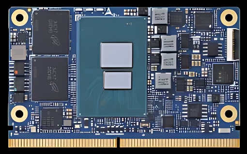
- The Standard Module Advanced RISC Computer defines an open standard for ARM-based embedded computer modules.
- Utilizes a 314-pin MXM connector, addressing high-performance and low-power requirements.
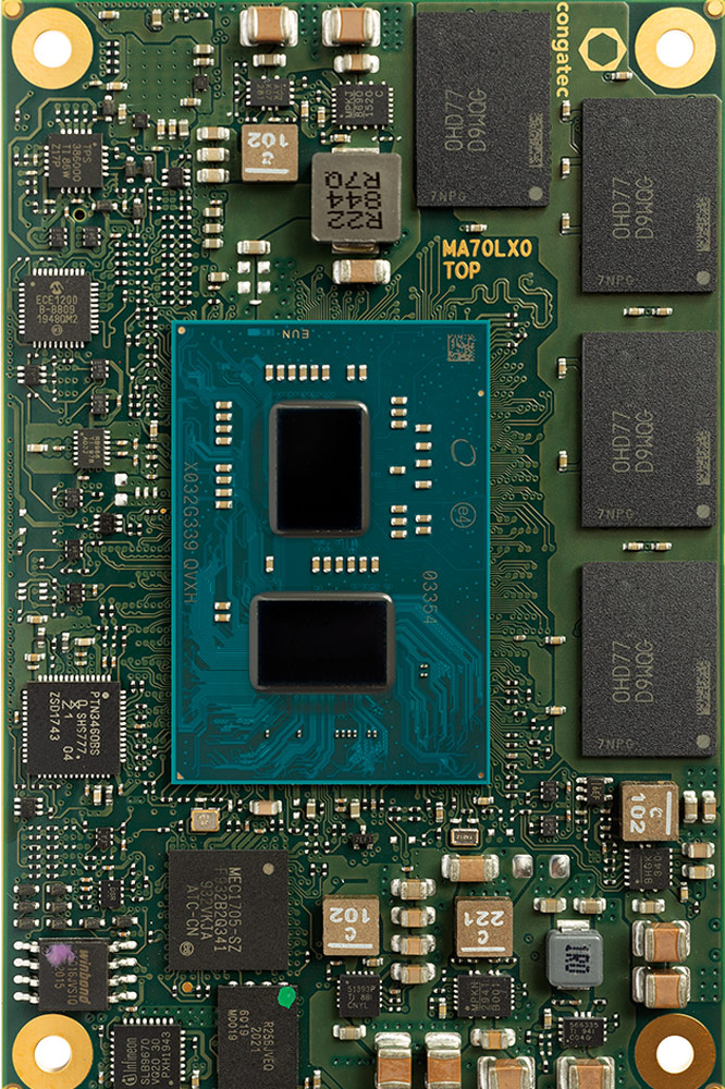
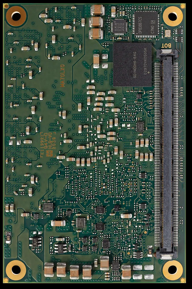
4. COM Express:
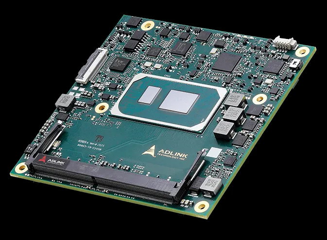
- Defined by the PCI Industrial Computer Manufacturers Group (PICMG), it supports various processor architectures like x86, ARM, and PowerPC.
- Offers three module sizes: Mini, Basic, and Compact, tailored to application and power needs.
- Recent updates in COM Express R3.1 include support for PCIe Gen 4, USB 4.0, and 10G Ethernet upgrades for AIoT applications.
PCB Design of Embedded Core Boards
With the increasing performance of embedded processors and faster memory rates, PCB designs for core boards have evolved from 4-layer to 8–12-layer configurations. These advancements demand materials with reduced signal loss. Here are the key design steps:
1. Component Placement:
Standardized shapes and interfaces restrict layout variations.
The typical approach involves CPU reference manual guidelines, optimal fanout design, and strategic placement of CPU, DDR, and Flash, followed by power and auxiliary components.
2. Determining PCB Thickness:
- Common PCB thicknesses range from 0.5mm to 6.4mm.
- Design standards often specify thickness, but for undefined cases, thicker boards improve structural reliability.
3. Layer Stack-Up and Functional Segmentation:
- Decide on the total layers, dividing signal, power, and ground planes.
- Ensure routing requirements, high-speed signal integrity, and power delivery needs are balanced while minimizing layer count.
4. Copper Thickness:
- Copper plane thickness affects power delivery.
- Inner signal layers typically use thinner copper (e.g., 0.5oz or 1oz) to allow precise etching, crucial for high-speed signals where the skin effect limits performance benefits of thicker copper.
5. Impedance Control:
- High-speed signals like single-ended 50Ω or differential 100Ω lines require strict impedance control.
- Factors like copper thickness, dielectric constant, trace width, and spacing must be meticulously tuned using EDA tools.
6. Via Structure Selection:
- High-density core boards often employ blind and buried vias to optimize routing space.
- However, these increase manufacturing complexity and cost. Designers should simplify via structures without compromising functionality.
7. Material Selection:
- FR-4 meets most requirements, but high-speed boards often use materials like Panasonic's Megtron4/6 for superior dielectric properties and minimal loss tangent.
- Smooth copper surfaces are critical for reducing impedance variation and ensuring signal integrity, especially above 5GHz.
8. Design for Manufacturability (DFM):
- All designs must align with manufacturing capabilities to avoid costly iterations.
SOMs revolutionize embedded designs by offering modularity and scalability. By adhering to standardized classifications and meticulous PCB design practices, manufacturers can achieve high reliability, reduced costs, and accelerated time-to-market.


