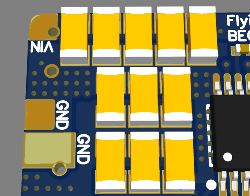
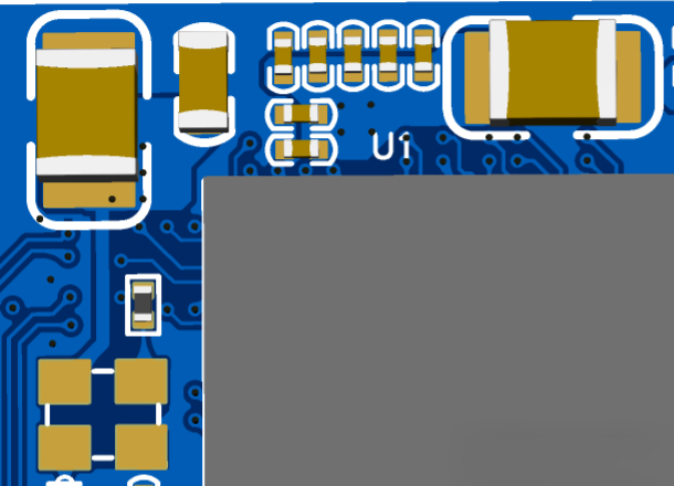
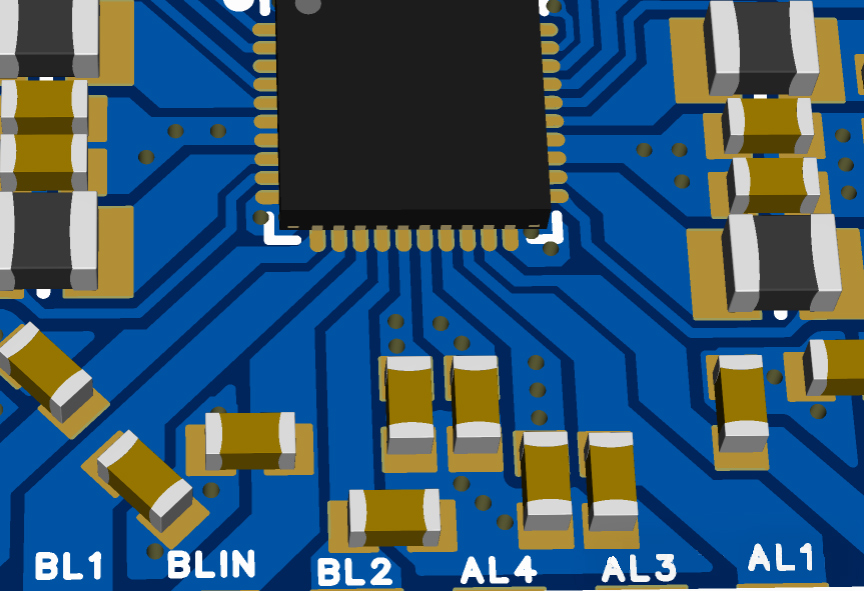
In PCB design, the strategic placement of capacitors plays a pivotal role in enhancing the circuit's performance, stability, and reliability, particularly in high-frequency and high-speed signal transmission applications. Properly positioned capacitors contribute to reducing noise interference, improving power integrity, and ensuring stable operation of active devices. This article discusses the various types of capacitors used in PCB designs, along with key placement guidelines based on their functional roles.
► Decoupling Capacitor Layout
Decoupling capacitors are crucial for maintaining a stable power supply by isolating power fluctuations and noise from the rest of the circuit. Here are some recommendations for effective decoupling capacitor placement:
1. Uniform Distribution: Decoupling capacitors should be evenly distributed around the chip to ensure comprehensive decoupling across the entire device.
2. Proximity to the Chip: Place the smallest capacitors closest to the chip, as these components typically have the highest resonance frequency and need to function within the shortest decoupling radius.
3. Role in Noise Suppression: Decoupling capacitors provide localized DC power to active components, helping to mitigate the propagation of switching noise and guide the noise to the ground. They function like a "battery," accommodating the fluctuating current demands of the driving circuit and minimizing mutual coupling interference between components.
► Filtering Capacitor Layout
Filtering capacitors are used to smooth out noise and ripple in the power supply, ensuring clean DC power is delivered to the circuit. The following guidelines should be followed when placing filter capacitors:
1. Proximity to Power Pins: Filter capacitors should be placed as close as possible to the power supply pins of the integrated circuits (ICs) to reduce impedance and minimize noise coupling along the power traces.
2. Location on Power Input: Typically, filtering capacitors are positioned at the power input stage to block high-frequency noise and interference coming from the power supply. These capacitors generally have larger capacitance values to handle significant ripple filtering.
3. Avoidance of High-Frequency Lines: To prevent high-frequency noise from degrading the filtering performance, filter capacitors should be kept away from high-speed signal traces, as these could induce unwanted electromagnetic interference (EMI).
4. Balanced Distribution: Filter capacitors can be distributed around the chip to balance power delivery and reduce supply voltage fluctuations.
5. Reducing Ripple: By smoothing AC ripple, filtering capacitors help improve the DC output by reducing alternating current ripple, which can otherwise interfere with sensitive electronic components.
► Bypass Capacitor Layout

Bypass capacitors are designed to redirect unwanted high-frequency noise from the power supply and provide clean power to the active components. Their placement is vital for effective noise suppression:
1. Power Line Placement: Bypass capacitors should be placed along the power line before the power enters the ICs, ensuring that the power supply is filtered before reaching sensitive areas of the PCB.
2. Capacitance Hierarchy: On the power line, start with a high-capacitance capacitor (e.g., 10µF) to handle lower-frequency noise and follow it with a smaller-value capacitor (e.g., 0.1µF) to filter higher-frequency noise.
3. High-Frequency Noise Filtering: Bypass capacitors effectively filter out the high-frequency components of the AC power signal. They create an alternate path for high-frequency currents, preventing them from interfering with sensitive areas of the PCB.
► Energy Storage Capacitor Layout

Energy storage capacitors are used to store and release energy rapidly as needed. They are typically larger in value and are vital in maintaining circuit stability during transient power demands. Here are key considerations for energy storage capacitor placement:
1. Capacitance and Size: Energy storage capacitors usually have larger capacitance values and, consequently, larger physical packages. They are designed to handle higher energy storage and release.
2. Proximity to Power Demands: While energy storage capacitors can be placed farther from active devices than decoupling or filtering capacitors, their placement should still allow quick energy delivery when needed. Ensure that they are not placed too far from components that require high-speed energy discharge.
3. Short and Direct Current Paths: The current path between the energy storage capacitor and the load should be as short and direct as possible to minimize energy loss and ensure efficient power delivery.
4. Rapid Energy Release: When other components in the circuit experience a sudden need for power, energy storage capacitors can quickly release stored energy to meet the demand, preventing voltage drops or power shortages.
Key Points on Capacitor Layout in PCB Design
1. Decoupling Capacitors: These should be placed evenly around the chip, with smaller capacitors closest to the chip to effectively isolate high-frequency noise and ensure stable operation.
2. Filtering Capacitors: Filter capacitors should be positioned near power pins to smooth out voltage fluctuations and noise. Larger capacitors handle low-frequency noise, while smaller ones manage high-frequency interference.
3. Bypass Capacitors: Placed along the power line to filter high-frequency noise, bypass capacitors prevent interference from reaching sensitive components by redirecting unwanted current away.
4. Energy Storage Capacitors: These large-value capacitors should be positioned to quickly supply energy when needed, with short current paths to reduce energy loss and ensure rapid discharge.


