
Introduction
PCBs (Printed Circuit Boards) are crucial for most modern electronic hardware, but they are susceptible to defects during the manufacturing process. These defects can lead to suboptimal PCBs that negatively impact product performance and the overall stability of quality. This guide delves into the major PCB manufacturing defects, explores their potential causes, and provides possible solutions for mitigating these challenges. A PCB consists of conductive copper traces laminated onto an insulating substrate, with components soldered to the board to form functional electronic circuits.
Throughout each manufacturing stage, defects can emerge, affecting the final product. Common defects include soldering issues, mechanical damage, contamination, dimensional inaccuracies, electroplating defects, misalignment of inner layers, drilling problems, and material issues. Addressing these defects is critical to maintaining high-quality standards and efficiency, as they can lead to electrical shorts, open circuits, poor aesthetics, reduced reliability, and total PCB failure. A deeper understanding of the primary causes of PCB defects enables manufacturers to implement robust process controls and inspection methods to minimize risk. Detecting and addressing defects early in the process is crucial for reducing scrap and avoiding functional issues in the final product. Close collaboration with PCB manufacturers and clear communication of quality and defect prevention expectations will yield positive results.
Main Causes of PCB Defects
Design flaws and manufacturing variations are the primary contributors to PCB defects. Below are some of the main causes of common PCB manufacturing defects:
1. Improper Design
Many PCB defects originate from design issues. Common design-related causes include inadequate trace spacing, small annular rings around drilled holes, sharp trace angles beyond manufacturing capabilities, and tolerances for fine lines or gaps that cannot be achieved in the manufacturing process.
Other issues include symmetrical patterns with a risk of acid traps, fine traces susceptible to electrostatic discharge, and potential heat dissipation concerns. Implementing comprehensive Design for Manufacturability (DFM) analysis and adhering to PCB design guidelines can prevent many design-related defects. Involving manufacturing engineers early in the design process helps evaluate manufacturability. Simulation and modeling tools can also verify the design's tolerance to real-world stresses and identify problem areas. Optimizing DFM is the key first step to minimizing common PCB manufacturing defects.
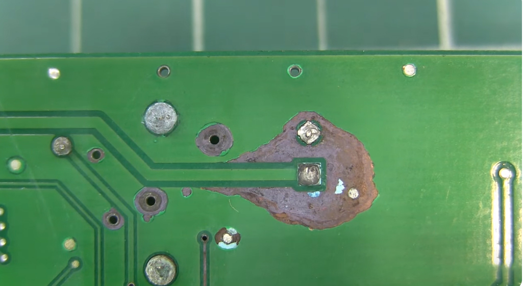
2. Contamination
PCB manufacturing involves many chemicals and processes that can lead to contamination. PCBs can easily be exposed to residues from solder flux, fingerprints, acid plating solutions, particulate debris, and cleaning agent residues. Contaminants can result in electrical shorts, open circuits, soldering defects, and long-term corrosion. Maintaining a clean production environment, implementing strict contamination controls, and preventing direct hand contact can help minimize contamination risks. Employee training on proper handling procedures is also essential.
3. Material Defects
The materials used in PCB manufacturing must be free from inherent defects. Substandard PCB materials, such as poor-quality laminates, prepregs, foils, and other components, may contain defects like insufficient resin content, fiberglass protrusion, pinholes, and nodules. These material defects can become embedded in the final board and affect performance. Ensuring all materials come from reputable suppliers with extensive quality control helps avoid material-related issues. It is also advisable to inspect incoming materials.
4. Mechanical Damage
PCBs are thin and fragile components susceptible to mechanical damage during manufacturing. Impacts, scratches, bending, dents, and other physical damage can occur. PCBs come into contact with many surfaces, fixtures, and handling equipment throughout production. Well-designed handling procedures and fixtures can minimize contact points, helping prevent mechanical damage. Proper training for employees in loading, moving, and storing PCBs is also important. Inspecting PCBs between process steps can help identify damage early.
5. Process Variations
Normal process variations can cause PCB defects if key parameters fall out of control. Common examples include inaccurate etching solution temperature, deviation in drilling speed, misalignment during lamination, and poor storage conditions. Using statistical methods to monitor processes allows for detection when deviations from required tolerances occur. Control charts provide a visual tool to keep the manufacturing process under statistical control, minimizing variation-related defects.
6. Human Error
Despite best efforts to prevent them, human errors remain inevitable in PCB production. Operators may mistakenly place PCBs into the wrong electroplating tanks, use incorrect drill bit sizes, improperly store finished boards, or make other errors that damage the PCB or cause defects. Comprehensive training programs, detailed work instructions, checklists, and increased automation help reduce human error. Redundancy measures such as secondary verification by machines can also catch errors before they affect the final product.


