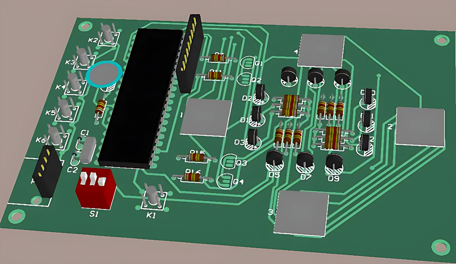
In everyday PCB design, engineers frequently encounter various spacing issues, such as the distance between vias and pads, the spacing between signal traces, and other critical measurements. These spacing requirements can be broadly classified into two categories: electrical safety spacing and non-electrical safety spacing.
► Electrical Safety Spacing
1. Trace-to-Trace Spacing:
The spacing between signal traces is one of the most fundamental design considerations in PCB layout. Based on the manufacturing capabilities of the PCB fabricator, the minimum trace-to-trace spacing should not be less than 4 mils (0.1 mm). This is also the minimum spacing for trace-to-trace and trace-to-pad distances. From a production perspective, it is always preferable to have larger spacing, provided the design allows it. For most designs, a typical trace-to-trace spacing of 10 mils (0.25 mm) is commonly used.
2. Pad Hole Diameter and Pad Width:
The pad hole size depends on the type of hole fabrication method used. For mechanically drilled holes, the minimum hole size should not be less than 0.2 mm. For laser-drilled holes, the minimum hole size should be no smaller than 4 mils (0.1 mm). Tolerances for hole diameters may vary slightly depending on the type of PCB material, but they are typically controlled within a tolerance of 0.05 mm. Regarding pad width, the minimum width should not be less than 0.2 mm.
3. Pad-to-Pad Spacing:
The spacing between adjacent pads is critical for ensuring proper soldering and manufacturing. According to PCB fabrication capabilities, the pad-to-pad spacing should be no less than 0.2 mm. The designer must also ensure that this spacing is sufficient for reliable manufacturing and subsequent assembly of components.
4. Copper-to-Edge Spacing:
For power-carrying copper pads (or copper pours), the spacing between the copper area and the edge of the PCB should ideally be at least 0.3 mm. In cases of large copper pours, there is typically an additional requirement for the copper to be inset from the edge of the PCB, usually by about 20 mils (0.5 mm). This is done to avoid issues such as edge damage, copper exposure that could cause short circuits, or bending. To achieve this, PCB engineers commonly use the "keep-out" layer at the edge of the board, ensuring copper pours are kept at a safe distance from the PCB's edge.
► Non-Electrical Safety Spacing
• Character Width, Height, and Spacing
Silkscreen markings on PCBs, including text and symbols, must adhere to specific width and height guidelines. Typically, a common rule of thumb is to use 5/30 mils or 6/36 mils for the character size. If the text is too small, it can become illegible or fuzzy when printed during the PCB fabrication process, which may impact the clarity of the design and subsequent assembly. Therefore, designers must balance the space available with the legibility requirements for silkscreen printing.
• Silkscreen-to-Pad Distance
Silkscreen markings mustn't overlap or cover pads. When silkscreen markings cover a pad, it can prevent solder from properly adhering to the pad during the soldering process, which can affect the quality of component mounting. To avoid this, PCB manufacturers typically require a minimum clearance of 8 mils (0.2 mm) between silkscreen and pads. A 4-mil clearance may be acceptable when PCB space is tight. However, if silkscreen accidentally overlaps with pads during design, PCB manufacturers will automatically remove the silkscreen from the pad areas during fabrication to ensure proper soldering.
• Mechanical Structure and 3D Height/Horizontal Spacing
The mechanical design of the final product must be considered when placing components on a PCB, particularly in terms of the 3D height and horizontal spacing of components. During the assembly process, it is crucial to verify that the components do not interfere with the mechanical structures of the device, such as the housing or other components. Therefore, designers should ensure that there is enough vertical and horizontal clearance between components and the PCB edges or other parts of the mechanical structure. Adequate spacing is essential to guarantee the proper fit of the PCB within the final product and to avoid any potential conflicts during assembly or product usage.
In PCB design, ensuring correct spacing is crucial for both electrical and mechanical performance. Electrical safety spacing, such as trace-to-trace, pad-to-pad, and copper-to-edge spacing, is necessary to prevent electrical issues, signal integrity problems, and short circuits. Non-electrical safety spacing, such as silkscreen-to-pad clearance and mechanical structure considerations, helps prevent issues during the manufacturing and assembly processes. By adhering to these spacing guidelines and ensuring proper design and fabrication practices, engineers can optimize the performance and manufacturability of their PCBs while minimizing potential errors and risks.
PCB designers should always consider the specific capabilities of their PCB manufacturers and the intended application of the final product when determining the appropriate spacing for each element on the PCB.


