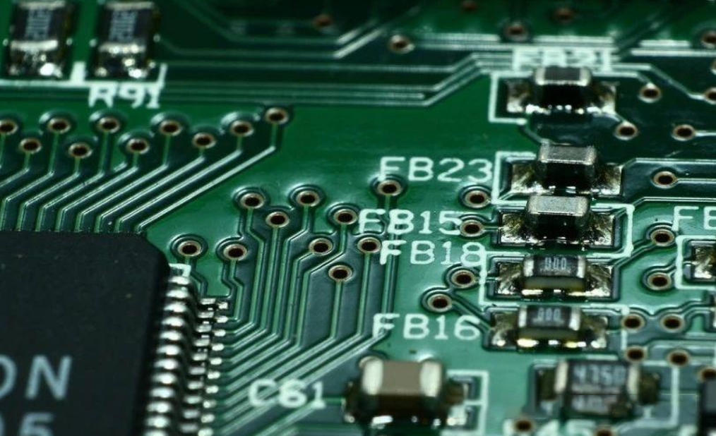
The PCB (Printed Circuit Board), an indispensable component in electronic devices, comprises multiple layers, each serving a distinct and critical function. Understanding the roles of these layers is pivotal for designing and fabricating high-quality PCBs. This comprehensive guide delves into the specifics of each layer, demystifying the complexity of PCB construction.
1. Signal Layers
At the heart of PCB functionality lies the signal layer, which is instrumental in transmitting electronic signals. Typically constructed from copper foil, signal layers undergo an etching process to form intricate circuit patterns. The number of signal layers varies based on the PCB's complexity; simpler designs may feature a single signal layer, whereas more sophisticated PCBs may incorporate multiple signal layers. These multi-layered configurations facilitate higher-density routing, enabling more complex circuit designs and higher-performance electronics.
2. Power Layers
Power layers are dedicated to distributing electrical power to the various components on the PCB. Similar to signal layers, they are composed of copper foil etched into power circuit patterns. The quantity of power layers correlates with the PCB's complexity, with simpler designs often utilizing a single layer and more intricate designs employing multiple layers. Proper power distribution is crucial for maintaining stable voltage levels and ensuring that all components receive adequate power without overloading.
3. Ground Layers
Ground layers provide a common reference point for electronic signals, offering grounding connections for components. Like signal and power layers, they are etched from copper foil into grounding circuit patterns. The number of ground layers depends on the PCB's complexity, aiming to establish a robust and low-impedance ground plane. This enhances electromagnetic compatibility (EMC) and electromagnetic interference (EMI) shielding, crucial for maintaining signal integrity and system reliability.
4. Solder Mask Layers
Solder mask layers serve as a protective barrier against oxidation and corrosion of the PCB's circuits. These layers are typically applied using green or other colored solder mask inks via a printing process. They cover the PCB surface, shielding the circuits from environmental contaminants and solder bridges during assembly. The solder mask also aids in component placement and soldering accuracy, enhancing PCB durability and longevity.
5. Silkscreen Layers
Silkscreen layers, often referred to as legend or overlay layers, are used for labeling and identifying electronic components and circuits on the PCB. They are printed with white or other colored inks, providing crucial information such as component values, polarity markers, and reference designators. This layer enhances PCB readability and ease of maintenance, facilitating accurate assembly and troubleshooting.
6. Additional Layers
Beyond the fundamental layers, PCBs may incorporate several other specialized layers to meet specific design requirements:
- Mechanical Layers: These layers define the PCB's physical dimensions and shape, guiding the manufacturing and assembly processes. They include outlines, mounting holes, and other mechanical features crucial for proper fit and function within electronic assemblies.
- Keep-Out Layers: Keep-out layers specify areas where no electrical traces or components should be placed, preventing short circuits and interference. They help ensure clearances and spacing are maintained, safeguarding circuit integrity.
- Internal Planes and Multilayer Configurations: PCBs with multiple layers often include internal planes for power and ground distribution, as well as additional signal layers. These configurations increase PCB integration, allowing for higher component density and superior performance. Advanced multi-layer stacking techniques, such as buried vias and blind vias, further enhance connectivity and design flexibility.
In conclusion, the interplay of these various layers constitutes the essence of a fully functional PCB. Each layer performs a unique role, collectively contributing to the PCB's overall performance, reliability, and manufacturability. Understanding these roles is fundamental for engineers tasked with designing and manufacturing PCBs, ensuring that they meet the rigorous demands of modern electronics. Whether it's optimizing signal integrity, managing power distribution, or facilitating ease of assembly and maintenance, the careful integration of PCB layers is key to delivering high-quality, reliable electronic products.


