
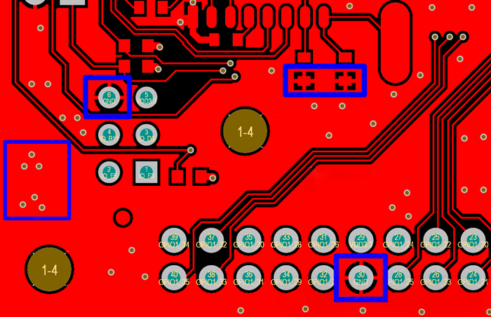
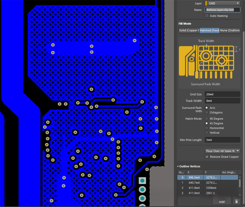
One critical final step in PCB design is copper pouring, which involves covering unused areas of the PCB with copper. Most PCB design software includes intelligent copper pour functionality, and the poured areas are typically highlighted in red to indicate copper coverage. Why is copper pouring the final step? Can't we skip it? For PCBs, copper pouring serves multiple purposes, such as reducing ground impedance, enhancing anti-interference capabilities, connecting to the ground to minimize loop area, aiding heat dissipation, and more.
Reducing Ground Impedance and Enhancing Noise Suppression
There are numerous spike pulse currents in digital circuits, making it essential to reduce ground impedance. Copper pouring is a common method to achieve this. By increasing the conductive cross-sectional area of the ground line, copper pouring reduces ground resistance. Alternatively, it can shorten the ground line length, decrease inductance, and thus lower impedance. It also controls the capacitance of the ground line, appropriately increasing its capacitance value to enhance conductivity and reduce impedance. Large-area copper pouring for grounds or power supplies can provide shielding, helping reduce electromagnetic interference, improve circuit anti-interference capabilities, and meet EMC requirements. For high-frequency circuits, copper pouring provides a complete return path for high-frequency digital signals, reducing DC network wiring and enhancing signal transmission stability and reliability.
Enhancing PCB Heat Dissipation
Apart from reducing ground impedance, copper pouring in PCB design also aids heat dissipation. As metals are good conductors of electricity and heat, copper-poured PCBs have more metallic components in gaps and other unused areas, increasing the heat dissipation surface area and facilitating overall PCB heat dissipation. Copper pouring helps distribute heat evenly, preventing localized high-temperature areas. Distributing heat evenly across the PCB reduces localized heat concentration, decreases the temperature gradient at heat sources, and improves heat dissipation efficiency. In PCB design, copper pouring can be utilized for heat dissipation through the following methods:
1. Designing heat dissipation areas: Based on the heat source distribution on the PCB, design appropriate heat dissipation areas and lay sufficient copper foil in these areas to increase the heat dissipation surface area and thermal conduction paths.
2. Increasing copper foil thickness: In heat dissipation areas, increasing copper foil thickness enhances thermal conduction paths and heat dissipation efficiency.
3. Designing thermal vias: Creating thermal vias in heat dissipation areas conducts heat to the other side of the PCB, increasing heat dissipation paths and efficiency.
4. Adding heatsinks: Installing heatsinks in heat dissipation areas transfers heat to the heatsinks, which then dissipate heat through natural convection or fan cooling, enhancing heat dissipation efficiency.
Reducing Deformation and Improving PCB Manufacturing Quality
Copper pouring helps ensure uniform plating and reduces deformation during lamination, especially for double-sided or multilayer PCBs, improving manufacturing quality. Uneven copper foil distribution across the board can lead to inconsistencies, which copper pouring effectively mitigates.
Meeting Special Component Mounting Requirements
For special components requiring grounding or specific mounting, copper pouring provides additional connection points and fixed support, enhancing component stability and reliability. Given these advantages, electronic designers often incorporate copper pouring into PCB designs. However, copper pouring is not always necessary in PCB design. In some cases, it may be unsuitable or infeasible. Examples include:
1. High-frequency Signal Lines: In high-frequency circuits, copper pouring may introduce additional capacitance and inductance, affecting signal transmission performance. It is often necessary to control the grounding trace routing and minimize the ground return path rather than excessively pouring copper. For instance, copper pouring around antenna sections can interfere with weak signal acquisition. Therefore, copper pouring is generally avoided in areas surrounding antennas.
2. High-density Boards: Excessive copper pouring on high-density boards may cause short circuits or grounding issues between traces, affecting circuit operation. When designing high-density boards, carefully design the copper pouring structure to ensure sufficient spacing and insulation between traces.
3. Excessive Heat Dissipation and Welding Difficulties: Full copper coverage on component leads may lead to rapid heat dissipation, making desoldering and repair difficult. High copper conductivity quickly dissipates heat during soldering, affecting welding quality. Therefore, designs should minimize heat dissipation using "cross-shaped pads" to facilitate welding.
4. Special Environmental Requirements: In high-temperature, high-humidity, or corrosive environments, copper foil may degrade or corrode, affecting PCB performance and reliability. In such cases, select appropriate materials and treatments based on specific environmental requirements instead of excessive copper pouring.
5. Special Layer Boards: For flexible circuits, rigid-flex boards, and other special-layer boards, copper pouring designs should adhere to specific requirements and design specifications to avoid issues arising from excessive copper pouring.
In PCB design, the choice between copper pouring and not pouring should be based on specific circuit requirements, environmental conditions, and special application scenarios.


