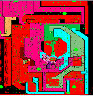
I. Considering PCB Design from the Perspective of Power Integrity
1. Decoupling Capacitor Layout
Decoupling capacitors play a crucial role in high-speed PCB design, and their placement is equally important. During short-term power supply from the power source to the load, the stored charge in the capacitor prevents voltage dips. Improper placement of capacitors can lead to excessive line impedance, affecting the power supply. Additionally, capacitors filter out high-frequency noise during high-speed switching of devices. Regarding decoupling capacitor placement, improper positioning can increase line impedance, reduce the resonant frequency, and affect the power supply. Small-value capacitors have short decoupling paths and should be placed close to ICs to be effective; large-value capacitors have longer decoupling paths and can be placed more flexibly. Therefore, the input power typically passes through large capacitors first, then small capacitors, before entering the IC chip.
2. Power Circuit Design
A well-designed power distribution network is essential to ensure power integrity. The design of power and ground lines should ensure widened widths to minimize impedance. As chip speeds increase, multilayer boards are increasingly used, with dedicated power layers for power plane segmentation and dedicated ground layers forming loops, reducing line inductance.
II. Considering PCB Design from the Perspective of Signal Integrity
PCB signal integrity issues include signal reflection, crosstalk, delay, and timing errors.
1. Reflection: When a signal travels on a transmission line, it reflects if the characteristic impedance of the transmission line does not match the source or load impedance, causing overshoot, undershoot, and ringing in the signal waveform. PCB design typically prevents reflection through impedance matching.
Single-ended: 50 ohms
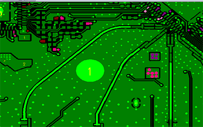
Differential: 100 ohms
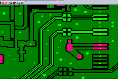
2. Crosstalk: In PCBs, crosstalk refers to undesired noise interference on adjacent transmission lines due to electromagnetic energy coupling through mutual capacitance and inductance. This occurs due to interactions between electromagnetic fields in the same area caused by different structures. Mutual capacitance causes coupling currents (capacitive crosstalk), while mutual inductance causes coupling voltages (inductive crosstalk). PCB design typically prevents crosstalk through the 3W rule or grounding shielding.
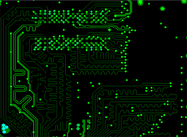
3. Signal Delay and Timing Errors: Signals travel at a finite speed on PCB traces, causing a transmission delay from the driver to the receiver. Excessive signal delay or mismatch can lead to timing errors and logical device malfunction, commonly occurring in DDR applications. PCB design typically mitigates signal delay and timing errors.
III. Considering PCB Design from the Perspective of EMC
EMC involves three main elements: interference sources, transmission paths, and sensitive devices. Design considerations focus on eliminating interference sources, cutting off transmission paths, and shielding sensitive devices.
1. Rational Layout
Related components should be placed close together in principle. Digital, analog, and power circuits should be separated, with high-frequency and low-frequency circuits also kept apart. Noise-prone devices, small-current circuits, and large-current circuits should be kept away from logic circuits. Key interference and radiation sources like clock circuits and high-frequency circuits should be arranged separately, far from sensitive circuits.
2. Shielding Design
Shielding is a key technology for solving electromagnetic compatibility issues. Electromagnetic shielding uses metal or magnetic materials to isolate electromagnetic interference from induction or radiation transmission from one area to another. It generally falls into two types: electrostatic shielding to prevent the impact of electrostatic fields and constant magnetic fields, and shielding to prevent the impact of alternating electric fields, alternating magnetic fields, and alternating electromagnetic fields.
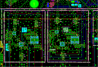
3. Stack-up Design
In general, stack-up design follows two rules: 1. Each trace layer must have an adjacent reference layer (power or ground); 2. Adjacent main power and ground layers should maintain a minimum spacing to provide significant coupling capacitance.

