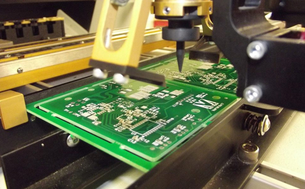
In PCB (Printed Circuit Board) design, ensuring proper spacing between copper traces, components, and the board's edge is critical for both electrical performance and product safety. Among the various spacing requirements, the PCB edge clearance, or board edge safety distance, plays a significant role in maintaining signal integrity, preventing dielectric breakdown, and achieving long-term reliability, particularly in high-density and high-voltage applications.
This article delves into the concept, influencing factors, calculation methods, and recommended guidelines for PCB edge clearance. Whether designing for consumer electronics, industrial systems, or defense-grade hardware, understanding and implementing proper edge spacing is fundamental.

1. Understanding PCB Edge Clearance
The PCB edge clearance refers to the minimum distance between any conductive element, such as a copper trace, pad, or component, and the edge of the PCB. This parameter is vital for:
- Preventing arcing or flashover at the edges
- Avoiding physical damage during fabrication or assembly
- Reducing electromagnetic interference (EMI)
- Complying with regulatory safety standards
Proper edge spacing enhances mechanical and electrical robustness, especially in multilayer and high-speed PCB designs.
2. Key Factors Affecting PCB Edge Clearance
Several critical factors influence how much clearance is needed between a trace/component and the PCB edge:
a. Dielectric Material Properties
The type of PCB substrate (e.g., FR4, Rogers, Polyimide) affects the dielectric strength and isolation performance. Materials with higher dielectric strength allow closer spacing, but safety margins must still be maintained.
b. Operating Voltage
As a general rule, higher operating voltages require greater edge clearance to avoid dielectric breakdown or arcing. IPC-2221 standards provide baseline recommendations for spacing based on voltage levels.
c. Product Category and Regulatory Requirements
Different applications come with different standards:
- Consumer electronics may allow tighter clearances
- Industrial and automotive systems often require increased spacing due to harsher environments
- Military and aerospace PCBs follow stringent MIL-spec requirements
d. Electromagnetic Compatibility (EMC)
Edge clearance impacts EMI and signal integrity. Maintaining proper spacing can help reduce edge radiation and signal coupling to adjacent circuits or metallic enclosures.
3. How to Calculate PCB Edge Clearance
Method 1: Standards-Based Estimation
IPC-2221 provides general spacing rules based on voltage levels. For example:
- Up to 30V: ≥ 0.13 mm (5 mils)
- 31V–100V: ≥ 0.6 mm (24 mils)
- Above 100V: Increase proportionally
These values offer a good starting point, but you should always factor in environmental conditions and reliability expectations.
Method 2: Field Simulation (FEM/EMC Tools)
Modern simulation tools like Ansys HFSS, CST Studio, or Altium's EM solver can analyze the electric field distribution near board edges. This helps optimize edge clearance without overdesigning and wasting board space.
4. Recommended Edge Clearance Guidelines
While clearance requirements vary, the following best practices can help ensure optimal design:
a. Minimum Distance from Copper to Edge
0.5 mm (20 mils) is a commonly used conservative value.
For high-voltage or high-reliability designs, consider 1 mm (40 mils) or more.
In routing layers, avoid placing traces too close to V-cut lines or panel edges to prevent delamination or shorts during depanelization.
b. Clearance for Mechanical Fixtures
If mounting holes, connectors, or screws are near the edge, increase spacing to avoid stress concentration and solder cracking.
c. Consider Fabrication Tolerances
Manufacturing processes such as routing, scoring, and punching introduce tolerances. A minimum of 0.25 mm to 0.5 mm is typically reserved to prevent copper exposure or shearing.
5. Safety, Reliability, and Compliance
In high-reliability applications, edge clearance is not just about electrical safety—it ensures long-term product stability and compliance:
UL Standards (e.g., UL 796): Define minimum spacing to prevent fire hazards.
IPC Standards: Provide layout guidelines for clearance based on voltage, environment, and class of the board.
CE and FCC EMC regulations: Indirectly impacted by poor edge design, leading to increased emissions.
6. Real-World Application Scenarios
Consumer Electronics
Devices like smartphones and wearables often have limited PCB real estate. Here, careful tradeoffs must be made between clearance and compactness. Simulation tools are essential for precision.
Automotive Electronics
Designs must withstand vibrations, moisture, and high temperatures. Edge spacing is widened to accommodate conformal coatings and reduce failure risks.
Industrial Equipment
High-voltage PCBs (e.g., motor drivers) need reinforced clearance and creepage distances, along with protective insulation layers or slots near board edges.
7. How PCBYES Ensures Optimal Edge Clearance
With more than 5 years in the field of PCB prototype and fabrication, PCBYES is committed to delivering reliable circuit designs that meet the highest quality standards. Our experienced engineering team evaluates edge clearance parameters in every project phase—from layout to final inspection—to ensure compliance and durability.
We utilize both IPC standard-based checks and advanced simulation tools to validate the safety margin of trace-to-edge distances. Whether you're designing a low-voltage controller board or a high-power inverter module, PCBYES ensures that every millimeter counts toward performance and safety.
8. Summary and Best Practices
To summarize:
PCB edge clearance is essential for electrical, mechanical, and regulatory reasons.
Clearance values depend on voltage, substrate, environment, and product category.
Always consult IPC standards and simulate when in doubt.
Design with manufacturing tolerances in mind to avoid post-production failures.
Partner with professional manufacturers like PCBYES, who understand how to implement precise spacing guidelines into mass production.
By optimizing edge clearance in your PCB layout, you can significantly enhance your product's performance, safety, and longevity.


