
1. Introduction
Electrostatic Discharge (ESD) is a critical Electromagnetic Compatibility (EMC) concern in PCB design, particularly in high-speed signal transmission, power management, and precision analog circuits. ESD events can lead to signal integrity degradation, component damage, or even system failure.
In electrostatic protection design, optimizing the ground grid (GND grid) layout is a key technique. A well-designed ground grid effectively mitigates the propagation of ESD energy, provides a low-impedance return path, and reduces electromagnetic interference (EMI). This article explores strategies for optimizing ground grid layouts to enhance the ESD resilience of PCBs, offering engineers practical guidelines for robust PCB design.
2. Impact of ESD on PCBs
ESD manifests as transient high-voltage and high-current pulses on the PCB, with the following characteristics:
- High voltage (hundreds to tens of thousands of volts): May cause dielectric breakdown in components.
- Short rise time (<1 ns): Disrupts high-frequency circuits and sensitive signal lines.
- High current (several to tens of amperes): Can burn PCB traces or solder joints.
Common ESD Coupling Mechanisms
- Direct discharge: ESD occurs when a human, tool, or device contacts PCB I/O ports, connectors, or exposed metal parts.
- Inductive coupling: ESD pulses couple into circuits through antenna effects or parasitic capacitance.
- Common-mode conduction: ESD enters the system via power or ground lines, impacting multiple circuit modules.
Key Methods to Mitigate ESD Effects
1. Enhancing PCB grounding systems to provide efficient ESD discharge paths.
2. Optimizing component placement and PCB layer stacking for improved signal integrity.
3. Deploying ESD protection components such as Transient Voltage Suppression (TVS) diodes at critical nodes.
3. Optimization of PCB Ground Grid Layout
3.1 Implementing a Grid-based Grounding Structure
The primary objective of a ground grid is to provide a low-impedance return path, minimize potential differences, and reduce high-frequency noise.
1. Design Principles of Ground Grid
- Grid pitch optimization: The grid spacing (Grid Pitch) should not exceed λ/20 (where λ is the wavelength corresponding to the dominant ESD pulse frequency), typically within 5–10 mm.
- Multipoint grounding: Ensures shorter and evenly distributed return paths for all signal nodes.
- Equal-potential design: Interconnect ground planes on different layers using stitching to reduce ground potential differences.
2. Advantages of Grid-based Grounding
- Establishes low-impedance paths to effectively direct ESD currents to ground.
- Reduces loop inductance in multipoint grounding configurations, minimizing common-mode noise.
- Distributes ESD energy, preventing localized PCB damage.
3.2 Via Optimization (Via Stitching)
Grid-based grounding relies on vias to interconnect ground planes across multiple layers. Optimizing via placement further enhances grounding effectiveness.
1. Via Spacing and Density
- Via spacing ≤ 5 mm to minimize local ground potential fluctuations.
- Higher via density in critical regions such as I/O ports, connectors, and keypads.
2. Selection of Via Types
- Through-hole vias: Commonly used for ground connections in multilayer PCBs.
- Blind vias: Suitable for High-Density Interconnect (HDI) PCBs, enabling compact designs.
- Filled vias: Minimize parasitic effects and improve high-frequency performance.
3.3 Grounding Optimization in Critical ESD Areas
1. I/O Port Regions
- Implement grid-based grounding near I/O ports and increase via density.
- Place TVS diodes between signal lines and ground to form a low-impedance discharge path.
- Use guard ring structures to improve ESD immunity.
2. Connectors and Metal Enclosures
- Ensure connector housings have low-impedance connections to the PCB ground plane.
- Apply shielding layers to reduce induced ESD interference.
- Place multiple ground vias near connector mounting holes to minimize contact resistance.
3. Keypads and Capacitive Touch Areas
- Utilize ground enclosure designs to prevent floating charge accumulation.
- Add ESD discharge paths, such as placing ground rings around keypads.
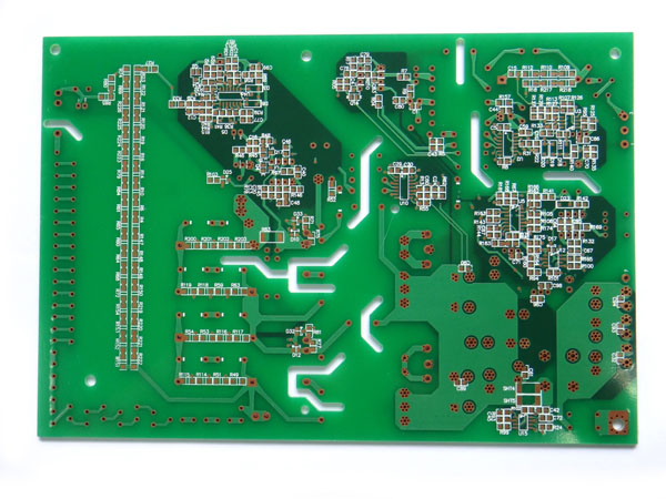
At PCBYES, we integrate these advanced grounding techniques into our PCB fabrication and assembly services, ensuring that our customers receive high-performance, ESD-resilient PCB solutions.
4. Testing and Simulation Validation
4.1 ESD Testing (IEC 61000-4-2 Standard)
- Contact discharge testing: Directly applies electrostatic stress to PCB critical areas to assess system stability.
- Air discharge testing: Simulates ESD effects from human interaction to evaluate circuit robustness.
4.2 High-Frequency Simulation (EMC Simulation Tools)
- Utilize Ansys HFSS and CST Studio to analyze the effects of ground grid structures on ESD mitigation.
- Simulate ESD pulse propagation under different grounding configurations to determine optimal layouts.
Optimizing ground grid layout is a fundamental technique for improving PCB ESD resilience. By implementing structured ground grids, strategic via placement, and targeted grounding enhancements in critical regions such as I/O ports, connectors, and touch-sensitive areas, engineers can effectively mitigate ESD risks.
Through rigorous ESD testing and simulation-driven design, PCBYES provides tailored PCB solutions that meet modern electronics' high-reliability demands. By integrating best practices in grounding optimization, we help our clients achieve superior EMC performance and robust product reliability.


