
In the development of electronic products, the ultimate goal of PCB design is to achieve circuit functionality and ensure efficient and reliable manufacturability. The process of optimizing design in conjunction with manufacturing is known as Design for Manufacturability (DFM). The core principle of DFM is to identify and eliminate design flaws that could lead to production issues, optimize product design to reduce manufacturing complexity, enhance yield rates, and minimize costs. This article explores key DFM principles in PCB design and how to implement them effectively.
Why is DFM Crucial in PCB Design? Neglecting DFM in PCB design may result in the following challenges:
- Higher Manufacturing Costs: Complex or suboptimal designs may require specialized processes such as multiple plating cycles or non-standard stack-ups, increasing production expenses.
- Lower Production Yield: Design flaws can cause issues during manufacturing, such as open circuits, short circuits, and soldering defects, leading to high scrap rates.
- Extended Lead Times: Design-manufacturing incompatibility may require multiple design revisions, increasing debugging time and delaying product launch.
By incorporating DFM principles from the outset, designers can optimize PCB layouts to minimize production challenges and improve efficiency and reliability.
Key DFM Principles in PCB Design
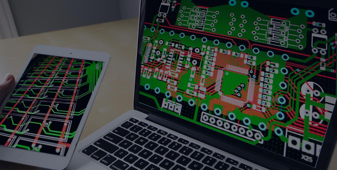
Design Rule Check (DRC)
DRC is a fundamental DFM tool that ensures a design meets the manufacturing capabilities of the PCB fabricator. Common DRC checkpoints include:
- Minimum Trace Width and Spacing: Ensuring signal traces and spacing meet fabrication tolerances, such as 6 mil/6 mil or smaller.
- Via Size: Adhering to the standard via hole diameters and annular rings, e.g., a minimum mechanical drill size of 0.2 mm and laser-drilled microvias as small as 0.1 mm.
- Pad-to-Hole Spacing: Preventing short circuits and electrical interference by maintaining adequate spacing.
- Best Practice: Collaborate with manufacturers early in the design phase and configure DRC settings in EDA tools based on their capabilities.
Optimizing PCB Stack-up A well-planned stack-up balances signal integrity and manufacturing cost while addressing mechanical strength and thermal management. Key considerations include:
- Layer Count: Minimize layer count to reduce costs while ensuring signal integrity and electromagnetic compatibility (EMC).
- Symmetry: Maintain a symmetrical stack-up to prevent PCB warpage due to thermal stress. For example, a 4-layer board can use a "signal-ground-power-signal" configuration.
- Copper Thickness: Choose appropriate copper thickness based on current requirements (e.g., 1 oz or 2 oz). Excessive thickness can complicate manufacturing.
- Best Practice: Utilize standardized stack-up configurations for high-density designs to avoid asymmetrical layouts.
Via Design Considerations Vias are critical for electrical connectivity in a PCB, but improper via design can lead to defects such as drill misalignment and poor plating. DFM guidelines for vias include:
- Annular Ring: Ensure annular ring width exceeds minimum requirements (typically 4-6 mil) to prevent drill misalignment issues.
- Via Filling and Tenting: Use filled vias or plugged vias in high-frequency or high-current applications to reduce resistance and prevent solder leakage.
- Via Spacing: Maintain sufficient via-to-via clearance to avoid drill damage.
- Best Practice: Use micro vias (blind/buried vias) in high-density designs to save space and improve reliability.
Component Pad and Placement Optimization
Proper component pad design is essential for high-quality soldering. Common issues include mismatched pad sizes and poor thermal pad design.
Pad Size Matching: Ensure pad dimensions align with component lead specifications to prevent poor soldering.
Thermal Pad Design:
- Add thermal vias in power component pads to enhance heat dissipation.
- Extend copper pours around power pads for better heat transfer.
Best Practice: Provide adequate test points under BGA and QFP components for post-assembly testing.
Signal Integrity and EMC Considerations
High-speed circuits require stringent signal integrity and EMC design to prevent manufacturing issues.
- Differential Pairs: Maintain consistent width and spacing while ensuring length matching.
- Shielding and Grounding: Place ground traces or shielding layers around critical signal paths to minimize noise.
- Return Path Optimization: Avoid routing signals over split ground planes to prevent discontinuities.
- Best Practice: Use simulation tools like HyperLynx for signal integrity validation and confirm design manufacturability.
Test Point Design
Test points facilitate electrical verification post-manufacturing. Good test point design enhances automation efficiency and reduces testing costs.
- Placement: Ensure accessibility for probes and avoid obstruction by components.
- Quantity: Optimize the number of test points while maintaining test coverage.
- Size: Use diameters compatible with testing equipment (e.g., ≥0.5 mm).
- Best Practice: For dense PCB layouts, consider flying probe testing but ensure test point positioning is optimal.
Panelization and PCB Array Design
PCB penalization directly affects manufacturing efficiency and cost.
- Panel Borders and Alignment Holes: Ensure sufficient border width (≥5 mm) and include fiducial marks for automated assembly alignment.
- Separation Methods: Choose appropriate breakaway techniques like V-CUT or Tab-Routing based on PCB shape.
- Routing Continuity: Ensure continuity in signal and power layers within panelized boards to prevent open circuits.
- Best Practice: Use Tab-Routing for irregular PCB shapes to minimize mechanical stress during separation.
Case Study: DFM Optimization in a High-Density Multilayer PCB
A communication device PCB with an 8-layer stack-up, multiple BGAs, and high-speed differential pairs initially faced manufacturing challenges:
- BGA Pad Spacing: Too close, resulting in high soldering defect rates.
- Differential Pair Mismatch: Causing poor signal integrity.
- Narrow Panel Borders: Hindering automated placement machine alignment.
Optimized Solutions:
- Increased BGA pad diameter and spacing to reduce soldering defects.
- Incorporated tuning regions in differential pair routing for precise length matching.
- Widened panel borders and standardized fiducial marks for accurate positioning.
- The improvements boosted yield rates to 98% and significantly reduced rework costs.
DFM is an essential aspect of PCB design that spans the entire development cycle from design to production. By adhering to DFM principles, designers can ensure circuit performance while optimizing manufacturability, reducing costs, and enhancing product reliability.
With more than five years of expertise in PCB prototyping and fabrication, PCBYES understands the importance of DFM and offers comprehensive solutions to help customers achieve high-quality, cost-effective PCB manufacturing. By closely collaborating with manufacturers and leveraging DRC and simulation tools, designers can achieve high-efficiency, reliable PCB production. At PCBYES, we are committed to delivering excellence in every aspect of your PCB needs.


